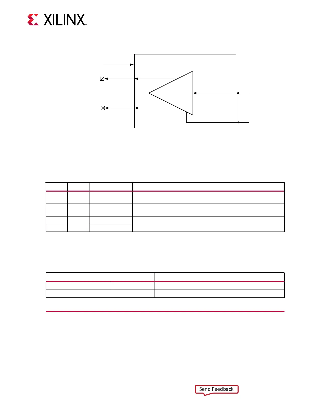
Figure 5: Reference Clock Output Use Model for OBUFDS_GTM
OBUFDS_GTM
MGTAVCC
GTREFCLKN
OB
O
GTREFCLKP
From RXRECCLK0/1
of GTM_DUAL
CEB
I
X20877-061418
Ports and Attributes
The following table denes the ports in the OBUFDS_GTM soware primive.
Table 5: Reference Clock Output Ports (OBUFDS_GTM)
Port Dir Clock Domain Description
CEB In N/A This is the active-Low asynchronous clock enable signal for the clock buffer.
Setting this signal High powers down the clock buffer.
I In (pad) N/A Recovered clock input. Connect to the output port RXRECCLK0/1 of the
GTM_DUAL primitive.
O In (pad) N/A Reference clock output port that gets mapped to GTREFCLKP.
OB Out N/A Reference clock output port that gets mapped to GTREFCLKN.
The following table denes the aributes in the OBUFDS_GTM soware primive that congure
the reference clock output.
Table 6: Reference Clock Output Attributes (OBUFDS_GTM)
Attribute Type Description
REFCLK_EN_TX_PATH 1-bit Reserved. This attribute must always be set to 1’b1.
REFCLK_ICNTL_TX 5-bit Reserved. Use the recommended value from the Wizard.
Reference Clock Selection and Distribution
The GTM transceivers in Virtex UltraScale+ FPGAs provide dierent reference clock input
opons. Clock selecon and availability is similar to the GTY transceivers in UltraScale+ devices,
but the reference clock selecon architecture supports only one LCPLL shared per Dual (two
GTM transceiver channels).
Chapter 2: Shared Features
UG581 (v1.0) January 4, 2019 www.xilinx.com
Virtex UltraScale+ GTM Transceivers 14
 Loading...

