Figure 54: Interfacing an LVPECL Oscillator to the GTM Transceiver Reference Clock
Input
LVPECL Oscillator
240Ω
240Ω
0.01 µF
0.01 µF
GTM Transceiver
Reference Clock
Input Buffer
Internal to
UltraScale+ Device
X20935-053118
Notes relevant to the gure:
1. The resistor values are nominal. Refer to the oscillator data sheet for actual bias resistor
requirement.
2. Before compleon of device conguraon, the terminaon resistor is not calibrated and the
voltage level input to the clock input buer should be made sure to not exceed the absolute
maximum rang as described in the UltraScale+ device data sheets (see hp://
www.xilinx.com/documentaon).
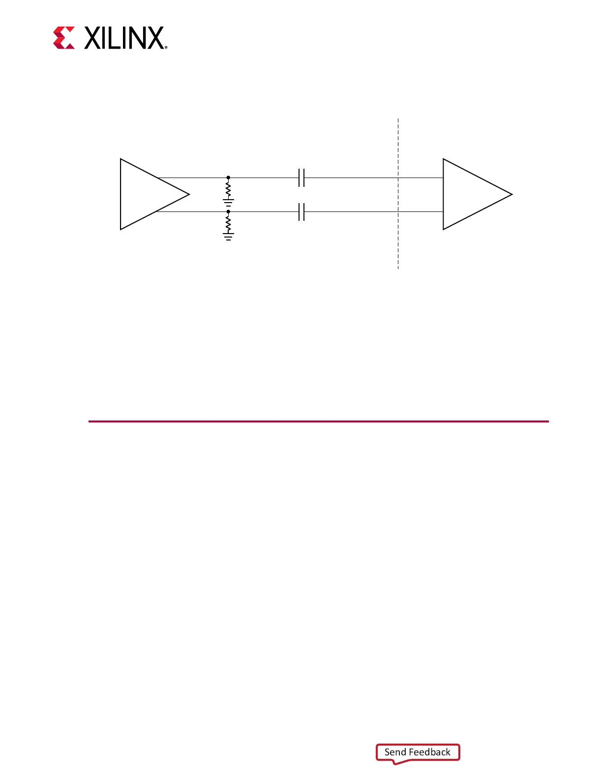
AC Coupled Reference Clock
AC coupling of the oscillator reference clock output to the GTM transceiver Dual reference clock
inputs serves mulple purposes:
• Blocking a DC current between the oscillator and the GTM transceiver Dual dedicated clock
input pins (which reduces the power consumpon of both parts as well).
• Common mode voltage independence.
• The AC coupling capacitor forms a high-pass lter with the on-chip terminaon that
aenuates wander of the reference clock.
To minimize noise and power consumpon, external AC coupling capacitors between the
sourcing oscillator and the GTM transceiver Dual dedicated reference clock input pins are
required.
Chapter 5: Board Design Guidelines
UG581 (v1.0) January 4, 2019 www.xilinx.com
Virtex UltraScale+ GTM Transceivers 124
 Loading...

