Use Mode External AC Coupling
Term
Voltage
(mV)
Suggested Protocols and Usage Notes
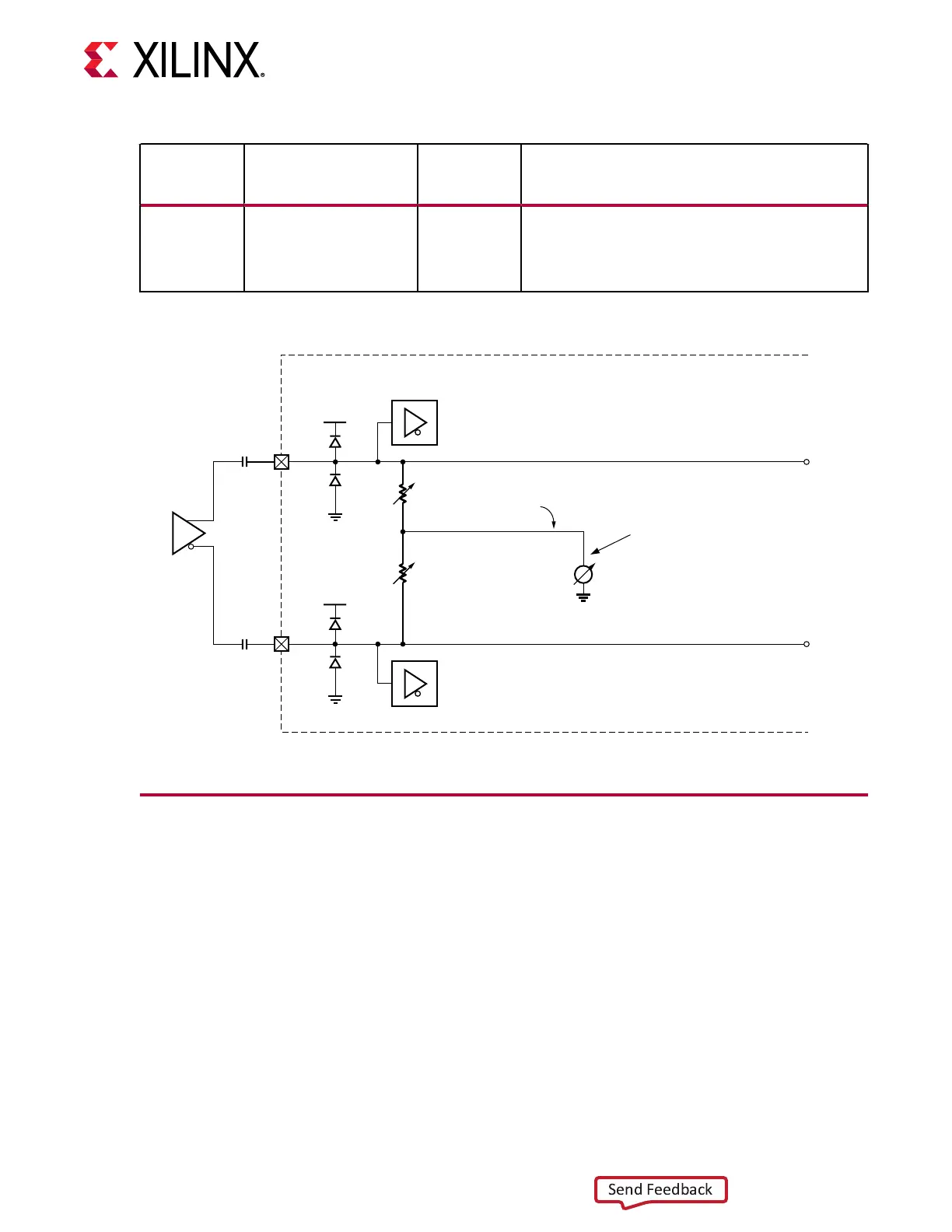
1 On 800 Attribute settings:
PAD_RTERM_VCOM_MODE = 2’b11
PAD_RTERM_VCOM_LVL = 4’b1010
Figure 38: Use Mode 1
+
–
UltraScale+ DeviceBoard
ACJTAG RX
ACJTAG RX
50Ω
50Ω
Programmable
MGTAVTT
MGTAVTT
~100 nF
~100 nF
PAD_RTERM_VCOM_MODE = 2'b11
PAD_RTERM_VCOM_LVL = 4'b1010
X20923-110518
RX Equalizer
A serial link bit error rate (BER) performance is a funcon of the transmier, transmission media,
and receiver. The transmission media of the channel is bandwidth-limited, and the signal traveling
through is subjected to aenuaon and distoron.
The GTM receiver is an ADC-based buer that breaks the equalizer into two domains: analog
and digital. The incoming signal rst passes through the analog stage consisng of a CTLE and
AGC stage. The signal is then digized by the ADC, and passes through the Feed-Forward
Equalizer (FFE) and Decision-Feedback-Equalizer (DFE), as shown in the following gure.
Chapter 4: Receiver
UG581 (v1.0) January 4, 2019 www.xilinx.com
Virtex UltraScale+ GTM Transceivers 87
 Loading...

