Proprietary Backplane Protocols with FEC up to 58 Gb/s
FEC can be enabled in 50G raw mode (with or without scrambling).
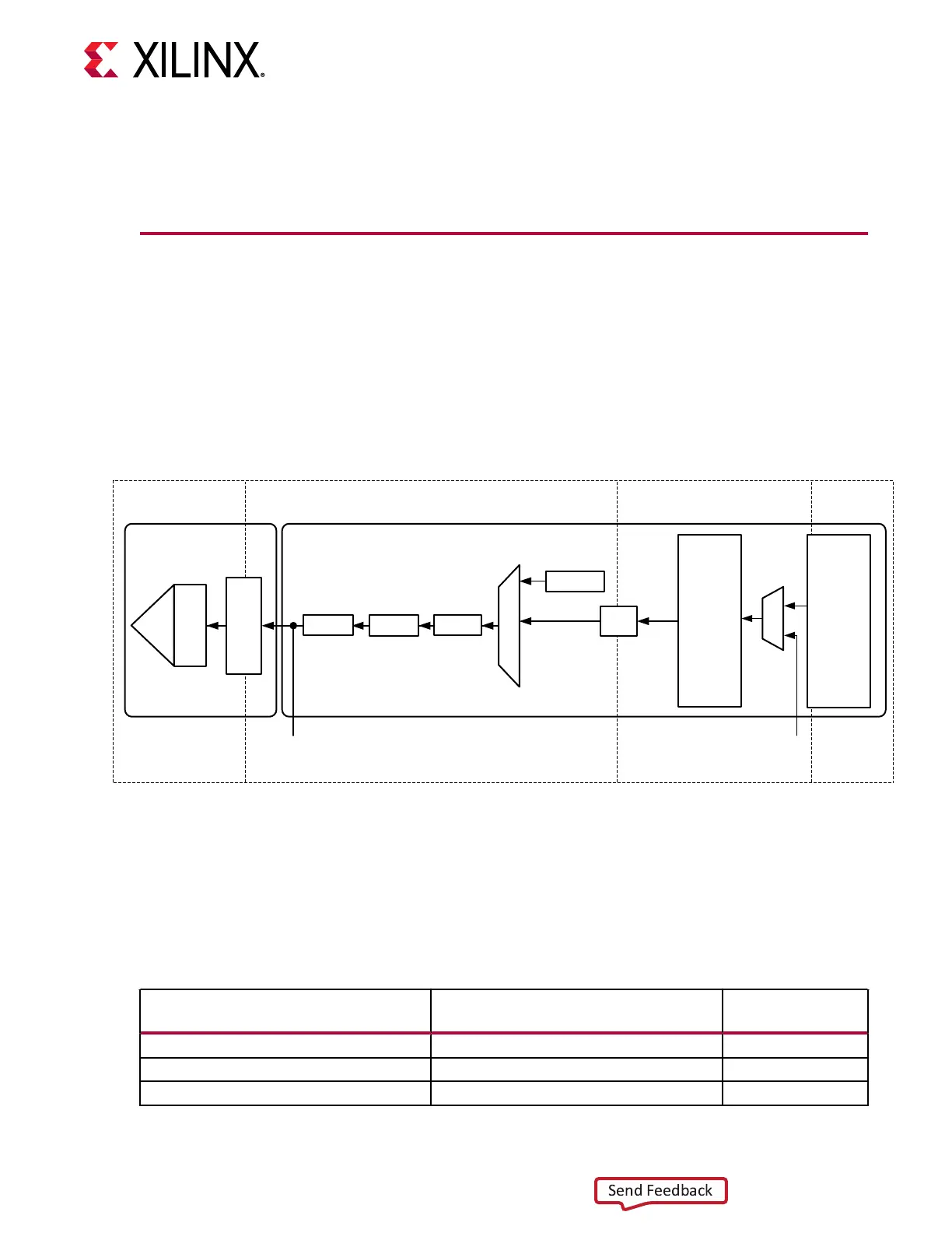
TX Buffer
The GTM transceiver TX datapath has two internal parallel clock domains used in the PCS: the
interface with PMA parallel clock domian (XCLK), and the PCS internal clock domain
(TXUSRCLK). To transmit data, the TX buer provides data width conversion between these
clock domains when necessary, depending on the operang data width and encoding mode. The
following gure shows the TX datapath clock domains.
Figure 30: TX Clock Domains
Pattern
Generator
Polarity
TX
FIFO
To RX Parallel Data
(Near-End PCS Loopback)
From RX Parallel Data
(Far-End PCS Loopback)
FEC
Gray
Encoder
TX PCS
PISO
TX
Driver
TX
Pre/
Pre
2/
Post
Emp
TX PMA
TX
Interface
TX Serial Clock PMA Parallel Clock (XCLK) PCS Parallel Clock (TXUSRCLK)
Device Parallel
Clock
(TXUSRCLK2)
X20914-053018
Pre-
Coder
The GTM transmier includes a TX FIFO to support data width conversion when data crosses
from TXUSRCLK to XCLK domain, and the table below shows the possible scenarios. The buer
does not tolerate ppm dierences, and only provides phase compensaon between the two
clocks. The TX buer inside the GTM transceiver must always be used. Buer bypass is not
allowed.
Table 34: TX FIFO Data Width Conversion Scenarios
PCS Parallel Clock (TXUSRCLK)
Domain Data Width
PMA Parallel Clock (XCLK) Domain
Data Width
FEC Support
64-bit 64-bit No
80-bit 128-bit Yes
128-bit 128-bit No
Chapter 3: Transmitter
UG581 (v1.0) January 4, 2019 www.xilinx.com
Virtex UltraScale+ GTM Transceivers 66
 Loading...

