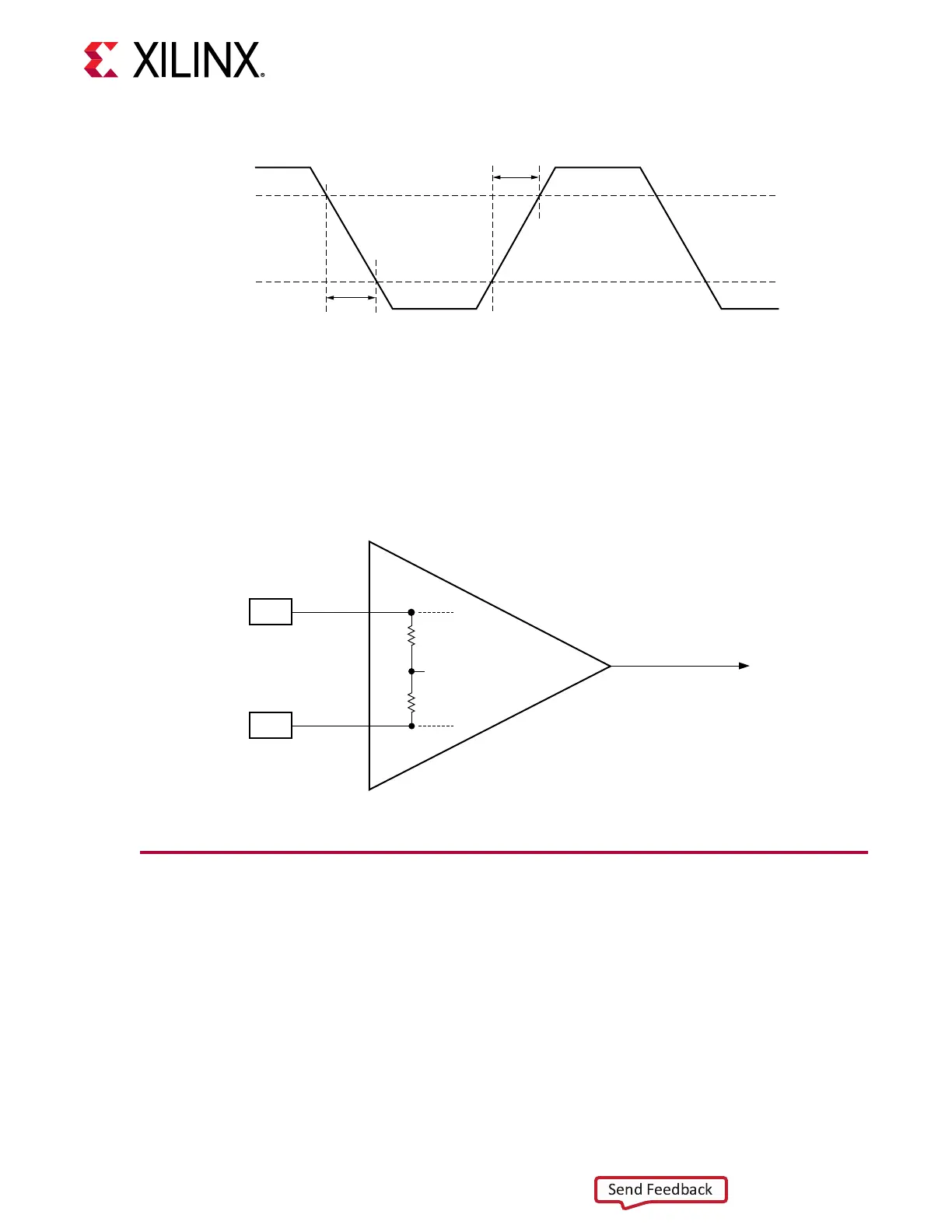
Figure 51: Rise and Fall Times
80%
20%
T
RCLK
T
FCLK
X20933-053118
The following gure illustrates the internal details of the IBUFDS. The dedicated dierenal
reference clock input pair MGTREFCLKP/MGTREFCLKN is internally terminated with 100Ω
dierenal impedance. The common mode voltage of this dierenal reference clock input pair is
4/5 of MGTAVCC, or nominal 0.8V for UltraScale FPGAs. The common mode voltage for
UltraScale+ FPGAs is MGTAVCC, or nominal 0.9V. See the UltraScale and UltraScale+ device
data sheets (see hp://www.xilinx.com/documentaon) for exact specicaons.
Figure 52: GTM Transceiver Board Design Guidelines
MGTREFCLKP
50Ω
50Ω
UltraScale+ FPGAs:
MGTAVCC
MGTREFCLKN
REFCLK
to GTM Transceiver
Dedicated
Clock
Routing
X21023-060718
GTM Transceiver Reference Clock Checklist
These criteria must be met when choosing an oscillator for a design with GTM transceivers:
• Provide AC coupling between the oscillator output pins and the dedicated GTM transceiver
DUAL clock input pins.
• Ensure that the dierenal voltage swing of the reference clock is the range as specied in the
UltraScale+ device data sheets (see hp://www.xilinx.com/documentaon). The nominal range
is 250 mV–2000 mV and the nominal value is 1200 mV).
Chapter 5: Board Design Guidelines
UG581 (v1.0) January 4, 2019 www.xilinx.com
Virtex UltraScale+ GTM Transceivers 122
 Loading...

