• Meet or exceed the reference clock characteriscs as specied in the UltraScale+ device data
sheets.
• Meet or exceed the reference clock characteriscs as specied in the standard for which the
GTM transceiver provides physical layer support.
• Fulll the oscillator vendor’s requirement regarding power supply, board layout, and noise
specicaon.
• Provide a dedicated point-to-point connecon between the oscillator and GTM transceiver
Dual clock input pins.
• Keep impedance disconnuies on the dierenal transmission lines to a minimum
(impedance disconnuies generate jier).
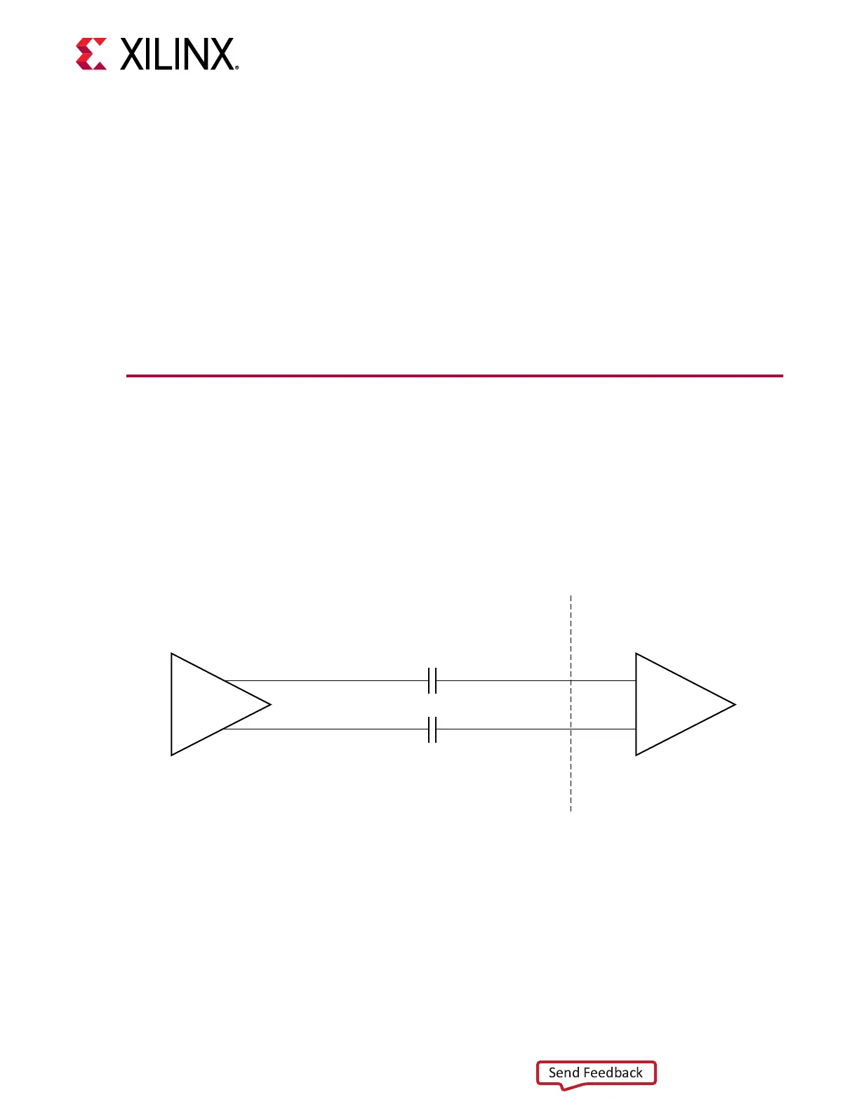
Reference Clock Interface
LVDS
The following gure shows how an LVDS oscillator is connected to a reference clock input of a
GTM transceiver.
Figure 53: Interfacing an LVDS Oscillator to the GTM Transceiver Reference Clock
Input
LVDS Oscillator
0.01 µF
0.01 µF
GTM Transceiver
Reference Clock
Input Buffer
Internal to
UltraScale+ Device
X20934-053118
LVPECL
The following gure shows how an LVPECL oscillator is connected to a reference clock input of a
GTM transceiver.
Chapter 5: Board Design Guidelines
UG581 (v1.0) January 4, 2019 www.xilinx.com
Virtex UltraScale+ GTM Transceivers 123
 Loading...

