• Output voltage swing
• Jier (determinisc, random, peak-to-peak)
• Rise and fall mes
• Supply voltage and current
• Noise specicaon
• Duty cycle and duty-cycle tolerance
• Frequency stability
These characteriscs are selecon criteria when choosing an oscillator for a GTM transceiver
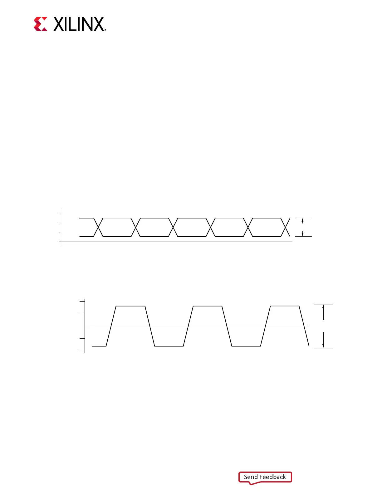
design. Figure 49 illustrates the convenon for the single-ended clock input voltage swing, peak-
to-peak. This gure is provided to show the contrast to the dierenal clock input voltage swing
calculaon shown in Figure 50, as used in the GTM transceiver poron of the UltraScale+ device
data sheets (see hp://www.xilinx.com/documentaon).
Figure 49: Single-Ended Clock Input Voltage Swing, Peak-to-Peak
+V
Single-Ended Voltage
0
MGTREFCLKP
MGTREFCLKN
X20931-053118
Figure 50 illustrates the dierenal clock input voltage swing, which is dened as MGTREFCLKP
- MGTREFCLKN.
Figure 50: Differential Clock Input Voltage Swing, Peak-to-Peak
+V
–V
0
MGTREFCLKP – MGTREFCLKN
V
IDIFF
X20932-053118
Figure 51 shows the rise and fall me convenon of the reference clock.
Chapter 5: Board Design Guidelines
UG581 (v1.0) January 4, 2019 www.xilinx.com
Virtex UltraScale+ GTM Transceivers 121
 Loading...

