Z8
®
CPU
User Manual
UM001604-0108 Serial Input/Output
120
Z8
®
CPU
hardware supports odd parity only, that is enabled by setting the Port 3 Mode
Register bit 7 to 1 (see Figure 112). If even parity is required, PARITY mode should be
disabled (P3M bit 7 set to 0), and software must calculate the received data’s parity.
Transmitter Operation
The transmitter consists of a transmitter buffer (SIO Register [F0h]), a parity generator,
and associated control logic. The transmitter block diagram is displayed as part of
Figure 105 on page 115.
After a hardware reset or after a character has been transmitted, the transmitter is forced to
a marking state (output always High) until a character is loaded into the transmitter buffer,
SIO Register (
F0h). The transmitter is loaded by specifying the SIO Register as the desti-
nation register of any instruction.
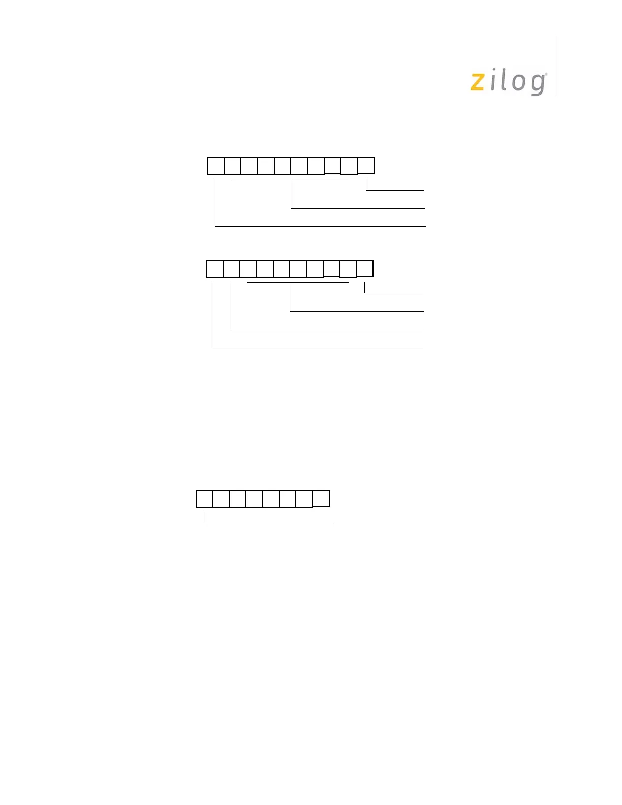
Figure 111. Receiver Data Formats
Figure 112. Port 3 Mode Register Parity
SP D7 D6 D5 D4 D3 D2 D1 D0 ST
Eight Data Bits
Start Bit
Start Bit
Seven Data Bits
One Stop Bit
SP P D6 D5 D4 D3 D2 D1 D0 ST
Parity Error Flag
One Stop Bit
Received Data
(No Parity)
Received Data
(With Parity)
D7 D6 D5 D4 D3 D2 D1 D0
(Write-Only)
0 = Parity OFF
1 = Parity ON
Port 3 Mode Register (P3M)
Register F7h

 Loading...