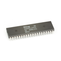
Z8
®
CPU
User Manual
UM001604-0108 External Interface
132
Data Strobe (Output, Active Low)—Data Strobe (DS) provides the timing for data
movement to or from the Address/Data bus for each external memory transfer. During a
Write Cycle, data out is valid at the leading edge of the DS
. During a Read Cycle, data in
must be valid prior to the trailing edge of the DS
.
Read/Write (Output)—Read/Write (R/W) determines the direction of data transfer for
memory transactions. R/W
is Low when writing to program or data memory, and High for
all other transactions.
Data Memory (Output)—Data memory (DM) provides a signal to separate external
Program Memory from external data memory. It is a programmable function on pin P34.
Data memory is active low for external data memory accesses and high for external Pro-
gram Memory accesses.
High Address Lines A15–A8—A15–A8 provide the High Address lines for the mem-
ory interface. The Port 0–1 mode registers must have bits D7 and D1 set equal to 1 to con-
figure Port 0 as A15–A8. Outputs can be CMOS- or TTL-compatible. Refer to product
specifications for actual type. See Figure 123 on page 133.
Address/Data Lines AD7–AD0—AD7–AD0 is a multiplexed Address/Data memory
interface. The lower eight Address lines (A7–A0) are multiplexed with Data lines (D7–
D0). Port 0–1 mode registers must have bits D4 set equal to 1 and D3 set equal to 0 to con-
figure Port 1 as AD7–AD0. Inputs and outputs are TTL-compatible. See Figure 123 on
page 133.
Reset—RESET
(input, active Low) initializes the Z8
®
CPU. When RESET is deacti-
vated, program execution begins from program location
000Ch. If held Low, RESET acts
as a register file protect during power-down and power-up sequences. To avoid asynchro-
nous and noisy reset problems, the Z8 CPU is equipped with a reset filter of four external
clocks (4T
P
C). If the external RESET signal is less than 4T
P
C in duration, no reset occurs.
On the fifth clock after the RESET
is detected, an internal reset signal is latched and held
for an internal register count of 18 or more external clocks, or for the duration of the exter-
nal RESET
, whichever is longer. Refer to specific product specifications for length of reset
delay time.
Crystal1, Crystal2 (Oscillator Input and Output)—These pins connect a parallel-
resonant crystal, ceramic resonator, LC, RC network, or external single-phase clock to the
on-chip oscillator input. Refer to the device product specifications for information on
availability of RC oscillator features.
External Addressing Configuration
The minimum bus configuration uses Port 1 as a multiplexed address/data port (AD7–
AD0), allowing access to 256 bytes of external memory. In this configuration, the eight
low-order bits (A0–A7) are multiplexed with the data (D7–D0).

 Loading...