Z8
®
CPU
User Manual
UM001604-0108 Power-Down Modes
112
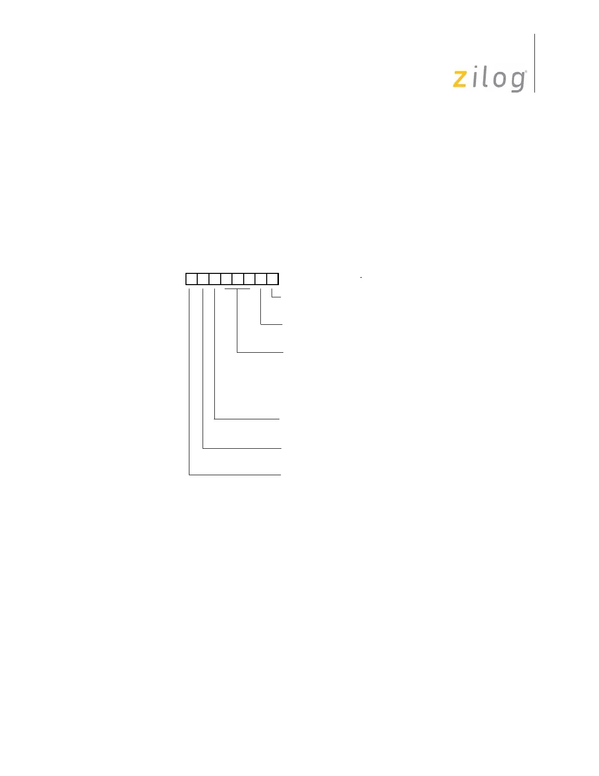
Stop Mode Recovery Register
This register selects the clock divide value and determines the mode of Stop Mode Recov-
ery (see Figure 103). All bits are Write-Only, except bit 7, that is Read-Only. Bit 7 is a flag
bit that is hardware set on the condition of stop-recovery and reset by a power-on cycle.
Bit 6 controls whether a low level or a high level is required from the recovery source. Bit
5 controls the reset delay after recovery. Bits 2, 3, and 4, of the SMR register, specify the
source of the Stop Mode Recovery signal. Bits 0 and 1 control internal clock divider cir-
cuitry. The SMR is located in Bank F of the ERF at address
0Bh.
The SMR register is available in select Z8 CPU products. Refer to the device product spec-
ification to determine SMR options available.
SCLK ÷ TCLK Divide-by-16 Select—This D0 bit of the SMR controls a divide-by-16
prescaler of SCLK ÷ TCLK. The purpose of this control is to selectively reduce device
power consumption during normal processor execution (SCLK control) and/or HALT
mode (where TCLK sources counter/timers and interrupt logic).
External Clock Divide-by-Two—This D1 bit can eliminate the oscillator divide-by-
two circuitry. When this bit is 0, the System Clock (SCLK) and Timer Clock (TCLK) are
equal to the external clock frequency divided by two. The SCLK ÷ TCLK is equal to the
Figure 103. Stop-Mode Recovery Register (Write-Only Except Bit D7, Which Is Read-Only)
D7 D6 D5 D4 D3 D2 D1 D0
SMR (Fh) 0B
Stop-Mode Recovery Source
000 POR Only and/or External Reset
001 P30
010 P31
011 P32
100 P33
101 P27
110 P2 NOR 0–3
111 P2 NOR 0–7
0 OFF **
1 ON
SCLK ÷ TCLK Divide-by-16
0 OFF
1 ON*
Stop Delay
0 POR*
1 Stop Recovery
Stop Flag (Read Only)
0 SCLK ÷ TCLK = XTAL ÷ 2*
External Clock Divide by 2
0 Low*
1 High
Stop Recovery Level
1 SCLK ÷ TCLK = XTAL
* Default setting after RESET.
** Default setting after RESET and Stop-Mode Recovery.

 Loading...