Z8
®
CPU
User Manual
UM001604-0108 Reset
36
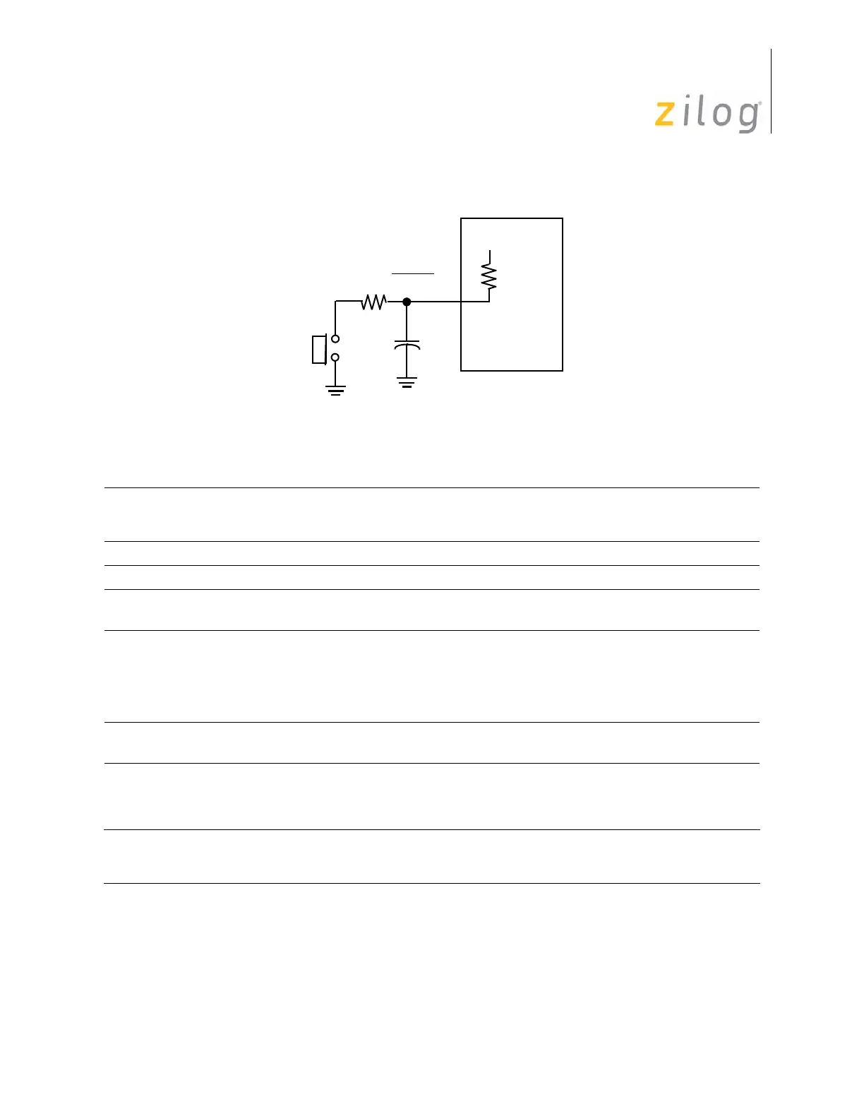
Figure 23. Example of External Power-On Reset Circuit
Table 13. ERF Bank 0 Reset Values at RESET
Register
(Hex) Register Name
Bits
Comments76543210
00 Port 0 UUUUUUUUInput mode, output set to push–pull.
01 Port 1 UUUUUUUUInput mode, output set to push–pull.
02 Port 2 UUUUUUUUInput mode, output set to open
drain.
03 Port 3 1111UUUUStandard digital input and output
Z86L7X Family Device Port P34-
P37 = 0
(Except Z86L70/71/75)
All other Z8 = 1.
04–EF General-Purpose
Registers 04h–EFh
UUUUUUUUUndefined.
Table 14. Sample Expanded Register File Bank C Reset Values
Register
(Hex) Register Name
Bits
Comments76543210
00 SPI Compare (SCOMP) 00000000
01 Receive Buffer (RxBUF) U U U U U U U U
02 SPI Control (SCON) U U U U 0 0 0 0
1 µF
+5V
100 KΩ
RESET
1 K
to
200 KΩ
10 V

 Loading...