Z8
®
CPU
User Manual
UM001604-0108 Z8
®
CPU Product Overview
2
default WDT clock source is an internal RC circuit (isolated from the device clock
source).
Auto Reset/Low-Voltage Protection—All family devices have internal Power-On Reset.
ROM devices add low-voltage protection. Low-voltage protection ensures the MCU is in
a known state at all times (in active RUN or RESET modes) without external hardware (or
a device reset pin).
Low-EMI Operation—Mode is programmable via software or as a mask option. This new
option provides for reduced radiated emission via clock and output drive circuit changes.
Low-Power—CMOS with two standby modes; STOP and HALT.
Full Z8
®
Instruction Set—Forty-eight basic instructions, supported by six addressing
modes with the ability to operate on bits, nibbles, bytes, and words.
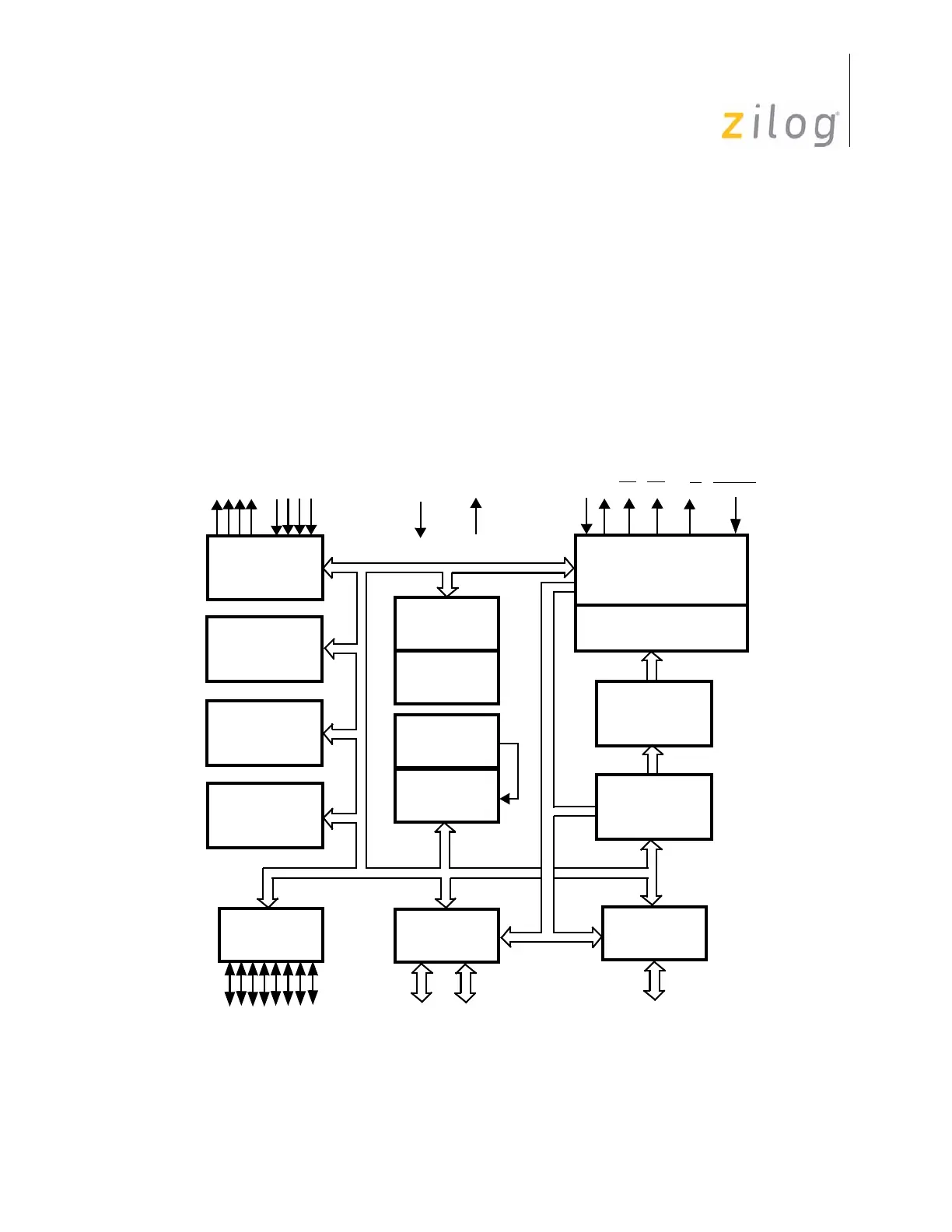
Figure 1. Z8 CPU Block Diagram
Port 3
Counter/
Timers (2)
Interrupt
Control
Analog
Comparators
(2)
Output
Input
ALU
FLAG
Register
Pointer
Register File
256 x 8-Bit
Machine Timing
& Instruction Control
RESET, WDT,
POR
Prg. Memory
512/K x 8-Bit
Program
Counter
V
CC
GND
XTAL
Address or I/O
(
Nibble
Programmable)
Port 2
Port 0
Port 1
AS DS
R/W RESET
44
8
Address/Data or I/O
(
Byte Programmable
)
I/O
(
Bit Programmable)

 Loading...