Debug
ARM DDI 0363G Copyright © 2006-2011 ARM Limited. All rights reserved. 12-13
ID073015 Non-Confidential
12.4.4 CP14 c0, Debug Self Address Offset Register
The DBGDSAR Register characteristics are:
Purpose Returns a 32-bit offset value from the Debug ROM Address Register to the
address of the processor debug registers.
Usage constraints The DBGDSAR Register is:
• in CP14 c0, sub-register c2
• a 32 bit read-only register
• accessible in User and Privileged modes.
Configurations Available in all processor configurations.
Attributes See Table 12-9.
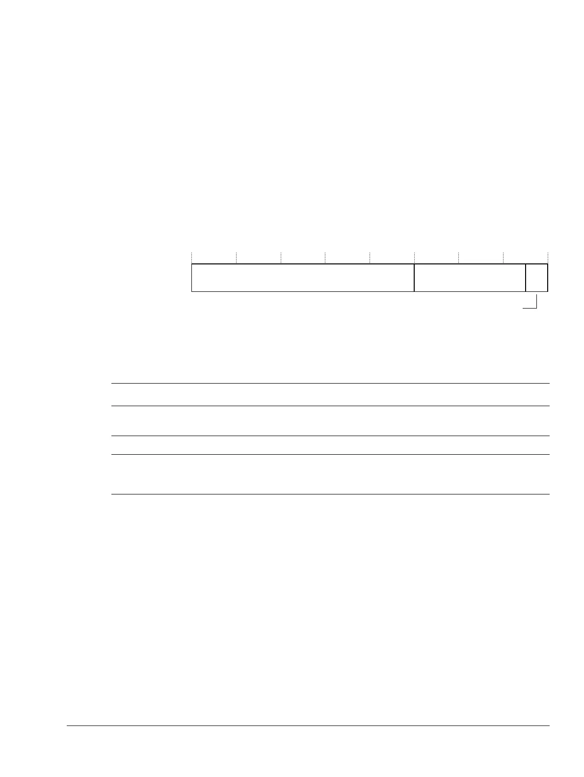
Figure 12-4 shows the DBGDSAR bit assignments.
Figure 12-4 DBGDSAR Register bit assignments
Table 12-9 shows the DBGDSAR bit assignments.
You can configure the address read in this register during integration using the
DBGSELFADDR[31:12] and DBGSELFADDRV inputs. DBGSELFADDRV must be tied
off to 1 if DBGSELFADDR[31:12] is tied off to a valid value.
To use the DBGDSAR Register, read CP14 c0 with:
MRC p14, 0, <Rd>, c2, c0, 0 ; Read DBGDSAR Register
Debug bus self address offset value Reserved
Valid bits
31 12 11 2 1 0
Table 12-9 DBGDSAR Register bit assignments
Bits Name Function
[31:12] Debug bus self
address offset value
Indicates bits [31:12] of the two’s complement offset from the debug ROM physical
address to the physical address where the debug registers are mapped.
[11: 2] - UNP on reads, SBZP on writes.
[1:0] Valid bits Reads b11 if DBGSELFADDRV is set to 1, otherwise reads b00.
DBGSELFADDRV must be set to 1 if DBGSELFADDR[31:12] is set to a valid
value.