Page 26
1) The programmer uses an internal 2.2kΩ pull-up
resistor on the data wire (SDA) when working with an
I2C device.
2) If the device to be programmed is 24LC(S)21A or
24LC(S)22A, its VCLK pin must be connected to VDD
during programming.
3) 34xx02 memory chips need “high” voltage at the A0
pin for commands protecting it against SWP and
CSWP recording. The “high” voltage is generated at
pin P, which must be connected to pin A0 in this
case. The memory chip pins A0, A1 and A2 must be
connected manually according to the selected
protection mode.
SPI Memory Chips
Fig.27: SPI memory chips
1) Some devices have WP, HOLD or RESET pins. All of
them must be connected to the required logic level in
such a way as not to block the communication or
device programming.
Different manufacturers mark the memory chips' SPI pins
with different names. Some of them are listed in the
following table:
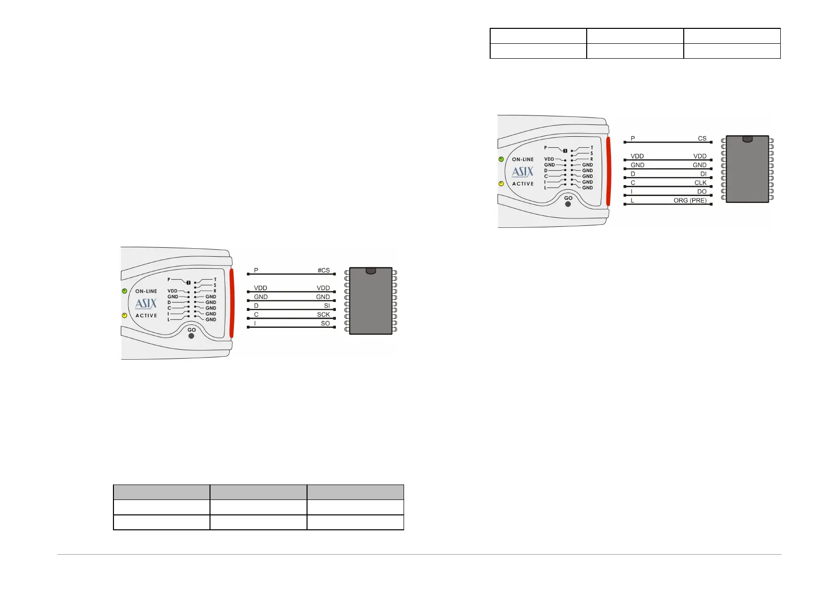
Microwire Memory Chips
Fig.28: Microwire memory chips
1) Pin L determines the memory organization as either
8-bits or 16-bits per word. The user selects the
required organization in the UP program and FORTE
then sets this pin to the corresponding logic level. If
this memory pin is firmly connected to the correct
logic level inside the application, pin L in the
programmer remains disconnected.
2) If used in combination with the M93Sx6 memory chip,
the programmer's L pin must be connected to the
device's PRE pin to serve for selecting the protection
register.