Page 28
5) ARM microcontrollers can be programmed from the
UP software through the JTAG interface.
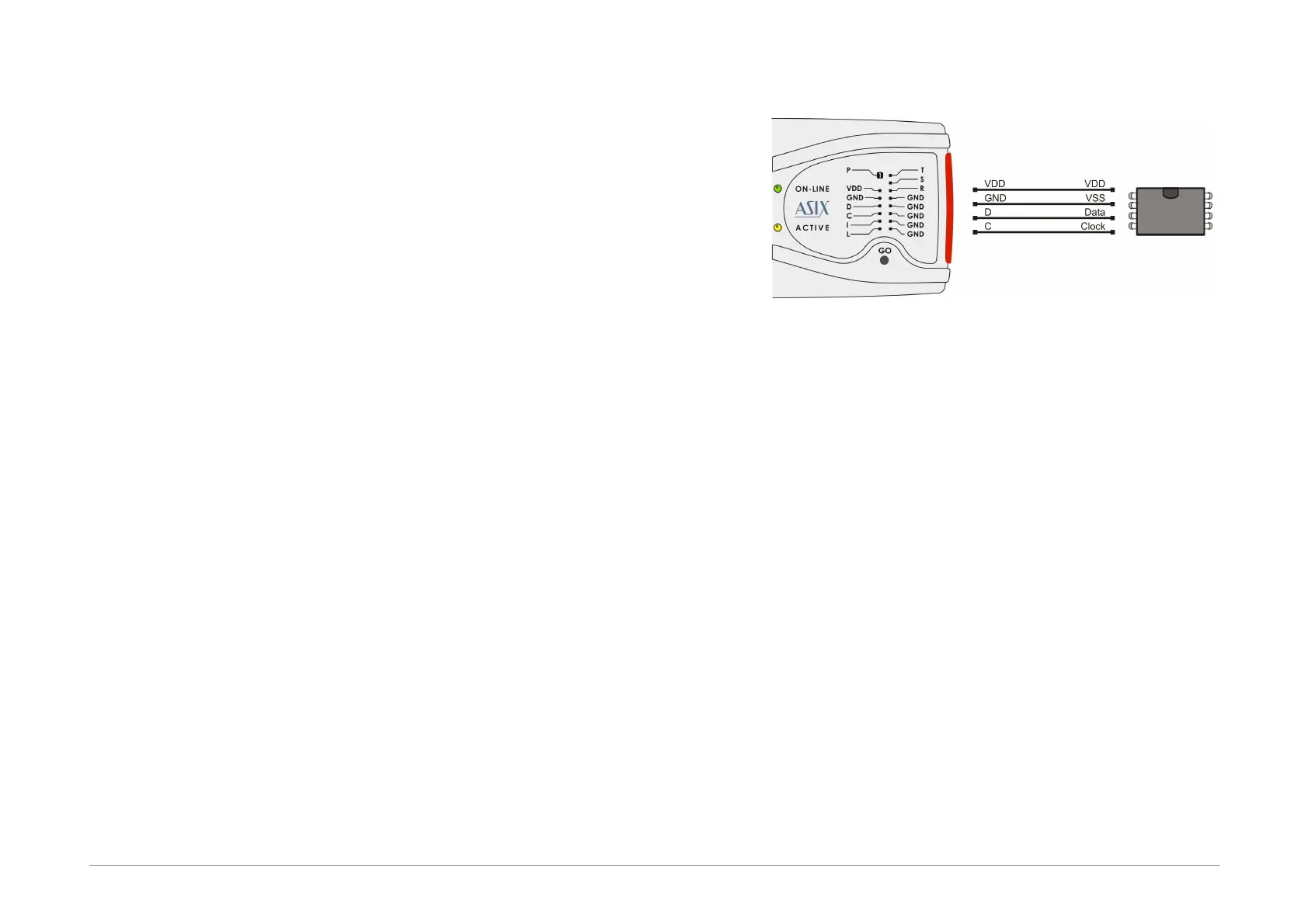
a) Devices which have SWD interface, e.g. most of
Cortex-M3 core chips, are programmed via this
interface, see its connection.
b) Clock source which is connected to the chip and its
frequency must be set in the FORTE programmer
settings window.
c) Using the programmer P pin is not mandatory for
the programming, but it should be connected to the
NRST pin of the device providing reset of the device
after programming to launch the application
program.
d) NXP LPC2xxx: For proper operation, it is required
to tie both /RESET and /TRST pins to FORTE P
output. Further, it is necessary to provide external
pull-down resistor of 4.7kΩ to 10kΩ on the /RTCK
pin. The LPC2xxx MCUs execute on-chip bootloader
after reset. The bootloader then examines pin P0.14
or P2.10 (depends on the part type, see the device
datasheet) to decide whether to start user
application on continue its operation (log.1 for user
application, log.0 for the bootloader). Because of
this, it is necessary to provide an external pull-up
resistor on this pin to start user programmed
application.
HCSxxx
1) The Clock signal is usually on S2 pin, the Data signal
is usually on PWM pin.