III-2
3.2 MAIN PCB
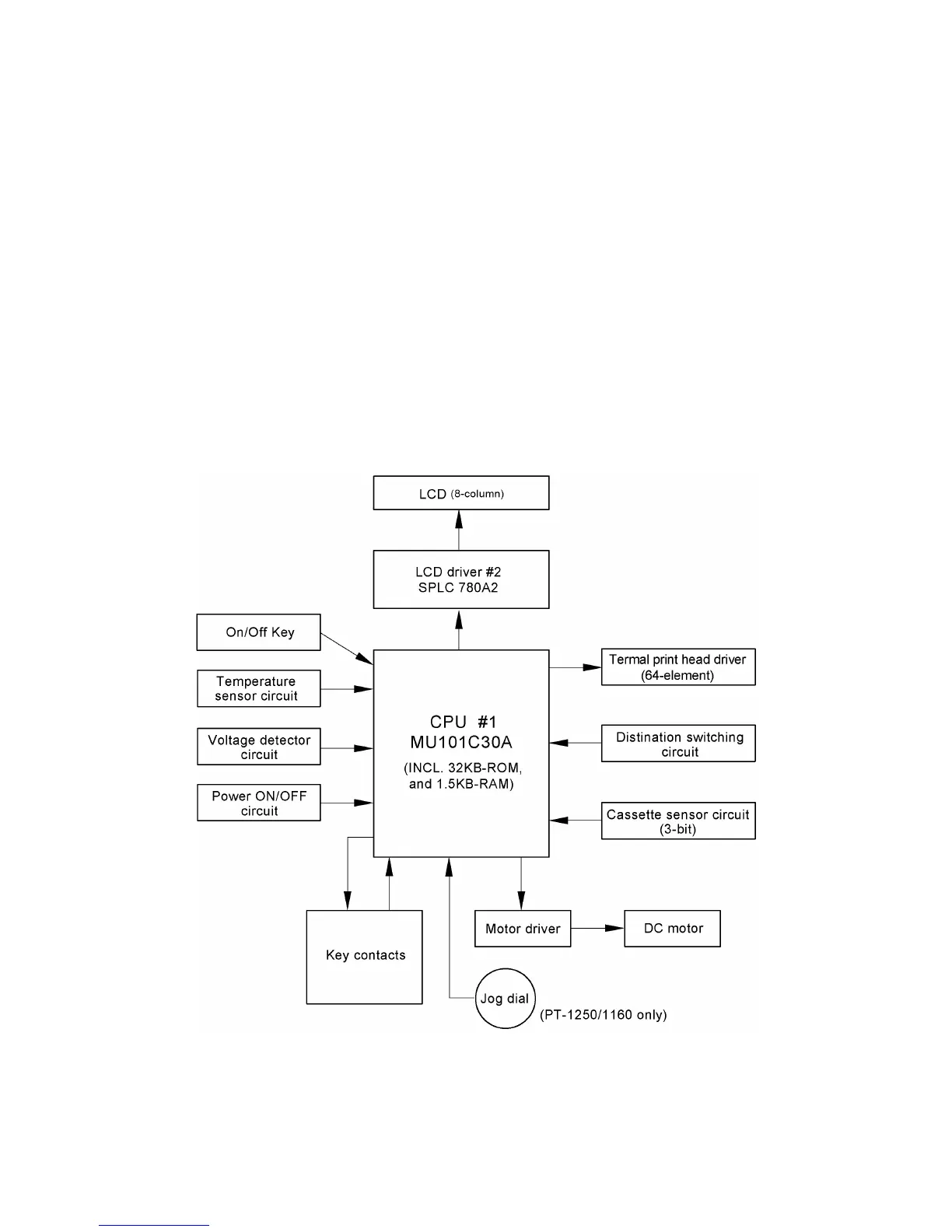
3.2.1 Main PCB Block Diagram
Fig. 3.2-1 shows the Main PCB block diagram. The PCB consists of the following:
(1) CPU (including a ROM, RAM, and LCD control)
(2) Key contacts matrix, solder points (specification switching-over circuit) and jog dial (PT-
1250/1160 only).
(3) Power On/Off circuit and power saving circuit
(4) Motor control circuit
(5) Thermal head drive circuit
(6) Voltage detection circuit and temperature sensor circuit
(7) Oscillation circuit
(8) Reset circuit
(9) Power supply circuit
(10) Cassette sensor circuit
Fig. 3.2-1 Main PCB Block Diagram

 Loading...