EPSON Stylus COLOR 860/1160 Revision C
Operating Principles Electrical Circuit Operating Principles 43
2.2.2 C298MAIN Board
The logic circuit of the C298MAIN is composed of the following:
n Logic line (CPU, ASIC, DRAM, EEPROM, and so on)
n Various motor control/driver circuits (CR motor, PF motor, and ASF/
Pump motor)
n Head control/driver circuits
n Interface control (parallel I/F, USB I/F)
n Sensor circuits
n Timer circuits
n Reset circuits
This main board is mainly different form other models in the following two
points.
o Use of the 3.3V chips in the logic circuit
The 3.3 V regulator (IC9) on the C298MAIN produces 3.3 V by pressuring
down the 5.5 VDC, also generated on this board, to drive several chips.
See the table below that separately shows the chips driven by the +5V and
+3V.
Table 2-10. 3.3V Drive Chips & 5.5V Drive Chips
o
Use of the slave CPU
Since the CR motor and PF motor of this printer are DC motors, the slave
CPU is attached on the main board in addition to the CPU and ASIC. This
slave CPU, serving to control the DC motors only, reduces duty of the CPU
and ASIC for faster data processing.
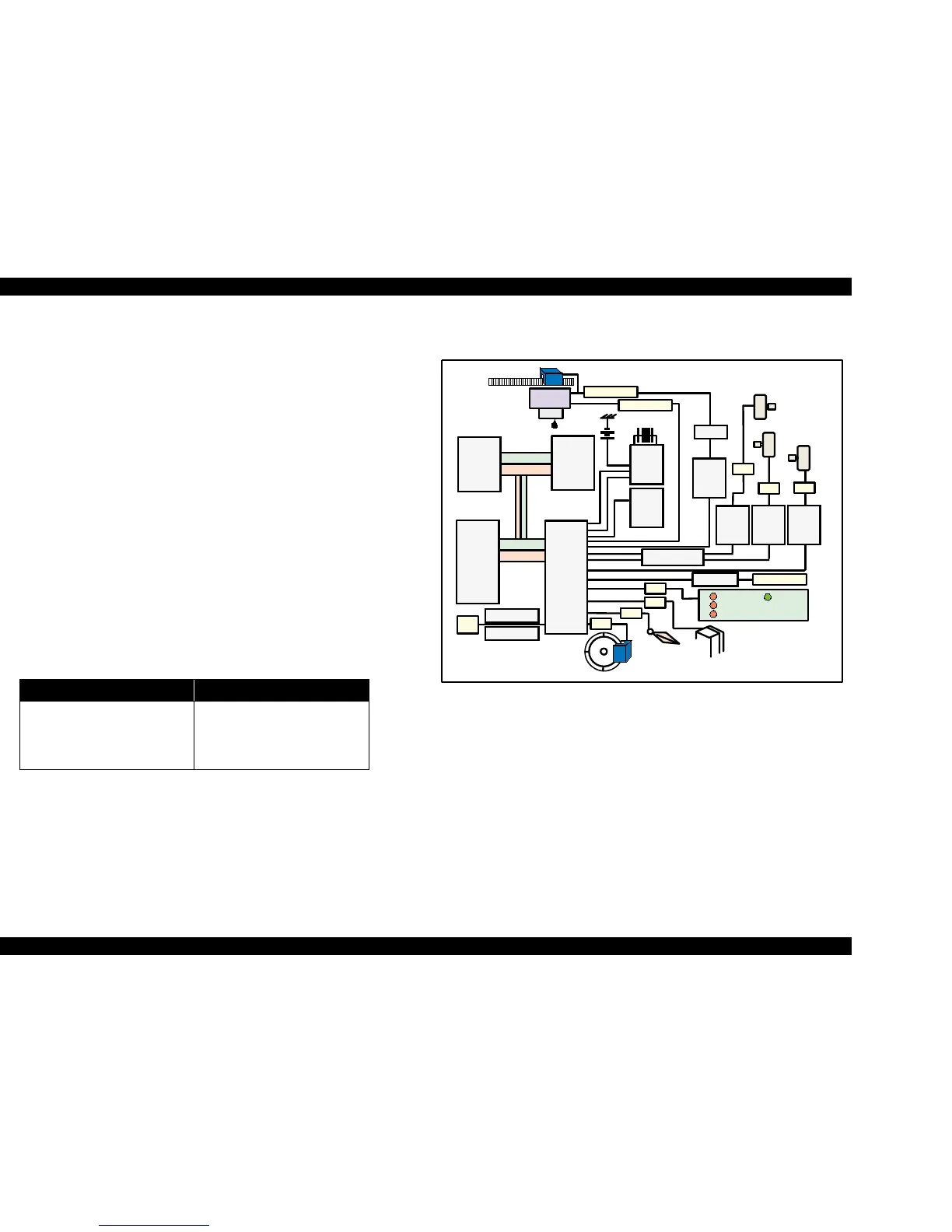
See Figure 2-16 for the C298MAIN board block diagram.
Figure 2-16. Block Diagram for the C298MAIN Board
+5V 3.3V
Sensors
I/F Circuit
PNL Board
Slave CPU
CPU
ASIC
P-ROM
D-RAM
C90A11CA
CPU (IC20)
Address
Data
Address
Data
CR1
Timer &
Reset IC
(IC5)
Batt1
EEPROM
(IC6)
CN1 Parallel
Common
Driver
(IC10 or
IC11)
Q3&Q4
CN8 HD FFC
Motor
Driver
(IC18)
Motor
Driver
(IC19)
PF Motor
CR Motor
CN14
CN13
C298 PNL (for SC860)
C303 PNL (for SC1100)
CN11
CN 6
ASF Sensor
CN5
PE Sensor
E05B70OD
ASIC (IC8)
D-RAM 16M
(IC3)
CN9 HD FFC
C90A120A
Slave CPU (IC15)
CN7
Motor
Driver
(IC12)
ASF/Pump Motor
P-ROM 16M
(IC2)
CN12
PF Encoder Sensor
Head
CR Encoder senser
IC4
74VHC1612B4
CN3
USB
IC7
IC21
E0BA13KA
PDIUSBF11A
 Loading...