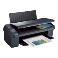
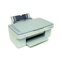
EPSON Stylus CX3500/CX3600/CX3650/CX4500/CX4600 Revision A
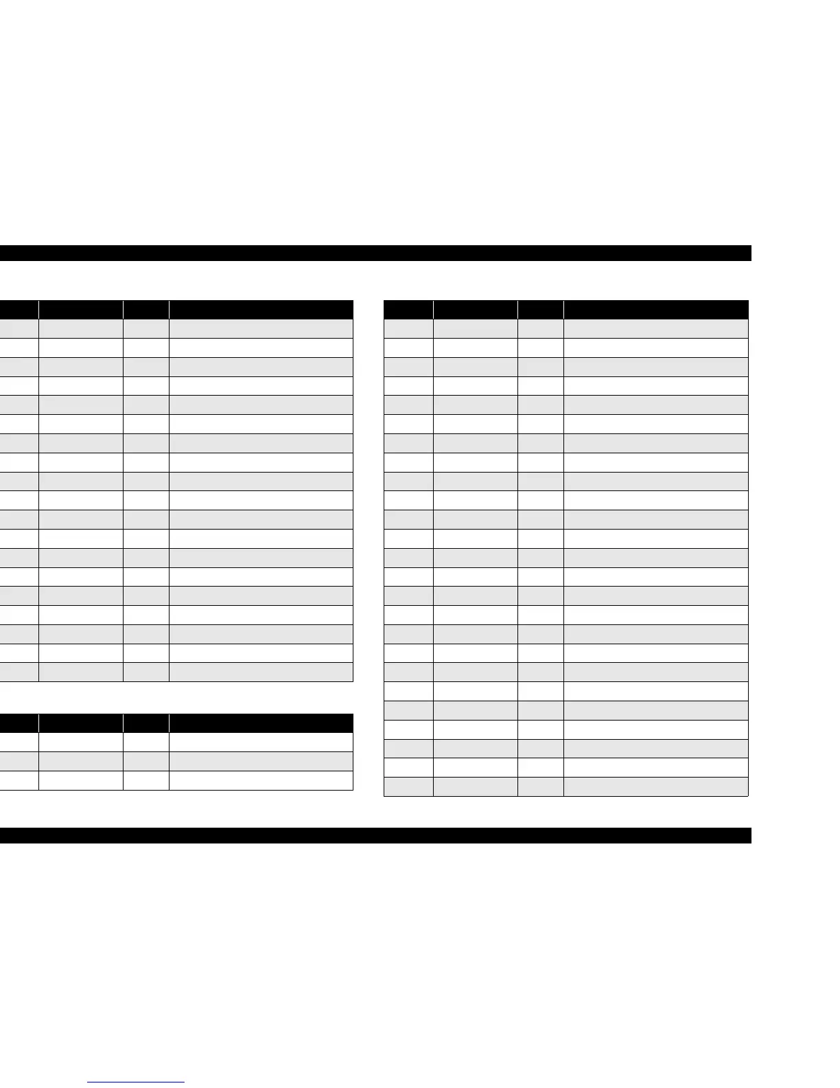
APPENDIX Connector Summary 186
32 /CE2 Card enable signal
33 NC/VS1 Voltage sensing 1
34 /IORD I/O read
35 /IOWR I/O write
36 /WE Write enable signal
37 RDY Ready
38 VCC — Power supply for CompactFlash
39 /CSEL — Not connected
40 RPU/VS2 Voltage sensing 2
41 RESET Reset
42 /WAIT Bus cycle extension
43 INPACK Input port response
44 /REG Register select
45 BVD2/SPKA Battery voltage detect/audio digital waveform
46 BVD1/STSCHG Battery voltage detect/card status change
47 CD8 Data bus for CF slot (8)
48 CD9 Data bus for CF slot (9)
49 CD10 Data bus for CF slot (10)
50 GND — Ground
Table 7-15. CN15 - Memory Card
Pin Signal Name I/O Function
1 GND — Ground
2 FCLE Command latch enable signal
3 FALE Address latch enable signal
Table 7-14. CN14 - Memory Card
Pin Signal Name I/O Function
4 FWEB Write enable signal
5 FWPB Write protect signal
6 FD0 SSFDC data (Bit 0)
7 FD1 SSFDC data (Bit 1)
8 FD2 SSFDC data (Bit 2)
9 FD3 SSFDC data (Bit 3)
10 GND — Ground
11 CD1 — Not connected
12 VCC — Power supply for SmartMedia
13 FD4 SSFDC data (Bit 4)
14 FD5 SSFDC data (Bit 5)
15 FD6 SSFDC data (Bit 6)
16 FD7 SSFDC data (Bit 7)
17 FLVD Low Voltage Detect
18 GND — Ground
19 FRDY Ready
20 FOEB Output enable signal
21 FCEB Chip enable signal
22 VCC — Power supply for SmartMedia
M1 GND — Ground
M2 BS Serial protocol bus state signal
M3 VCC — Power supply for MemoryStick
M4 SDIO Serial protocol data signal
M5 Reserve — Not connected
M6 INS Serial protocol data signal
Table 7-15. CN15 - Memory Card
Pin Signal Name I/O Function
 Loading...