EPSON Stylus CX3500/CX3600/CX3650/CX4500/CX4600 Revision A
APPENDIX Connector Summary 187
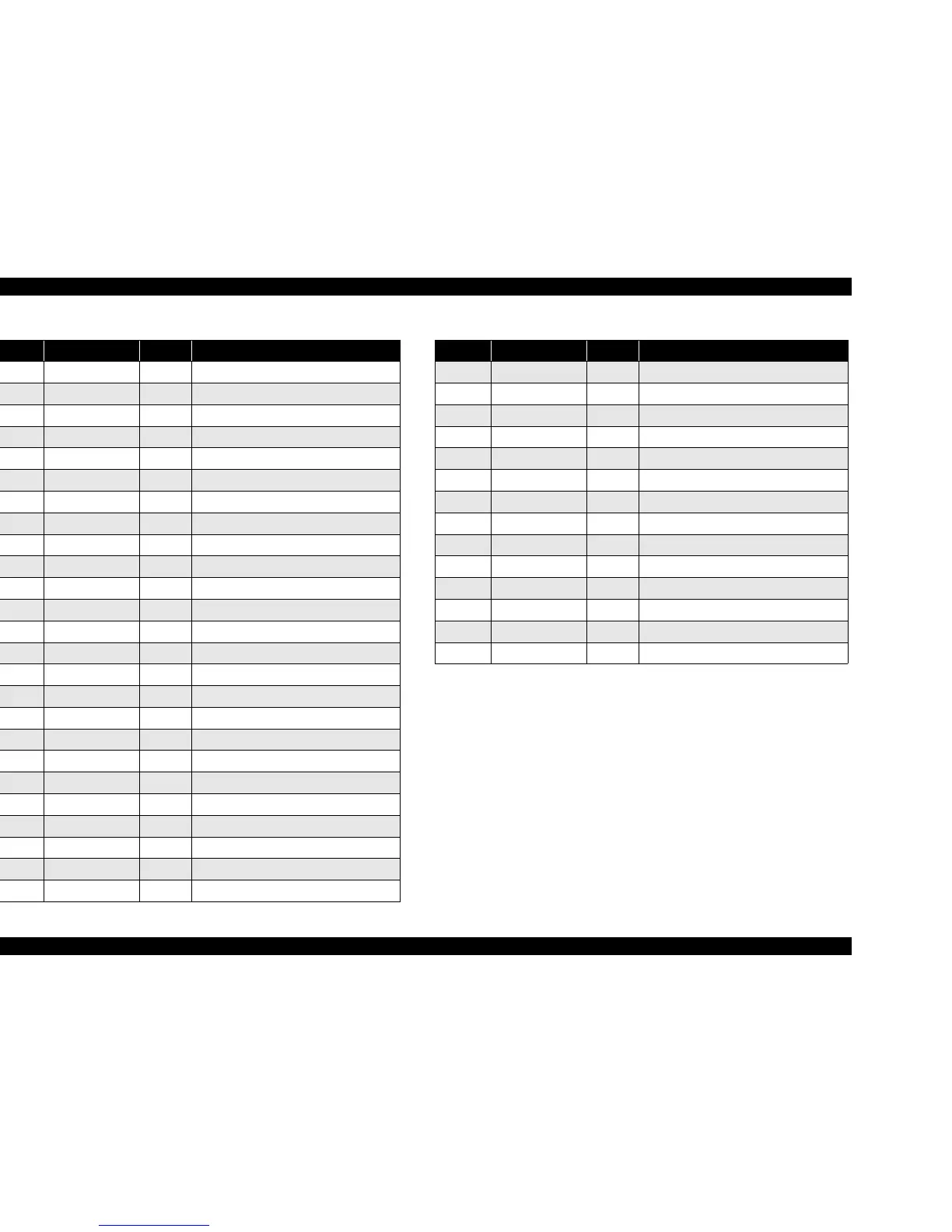
M7 Reserve — Not connected
M8 SCLK Stick inserted/removed detect terminal
M9 VCC — Power supply for MemoryStick
M10 GND — Ground
X1 GND — Ground
X2 XD_RDY Ready
X3 XD_OEB Output enable signal
X4 XD_CEB Chip enable signal
X5 XD_CLE Command latch enable signal
X6 XD_ALE Address latch enable signal
X7 XD_WEB Write enable signal
X8 XD_WPB Write protect signal
X9 GND — Ground
X10 XD_D0 XD data (Bit 0)
X11 XD_D1 XD data (Bit 1(
X12 XD_D2 XD data (Bit 2)
X13 XD_D3 XD data (Bit 3)
X14 XD_D4 XD data (Bit 4)
X15 XD_D5 XD data (Bit 5)
X16 XD_D6 XD data (Bit 6)
X17 XD_D7 XD data (Bit 7)
X18 XD_VCC — Power supply for xD-Picture Card
S1
WP
TBD
S2 SW_GND — Ground
S3 DETECT TBD
Table 7-15. CN15 - Memory Card
Pin Signal Name I/O Function
S4 CD Card detect signal
S5 GND — Ground
S6 WP1 Write protect seal condition
S7 GND — Ground
S8 XD_CD1 Card detect signal
D1 CD/DAT3 Card Detect /Data Line (Bit 3)
D2 CMD Command/Response
D3 GND — Ground
D4 VDD — Power supply for SD Memory Card
D5 CLK Clock
D6 GND — Ground
D7 DAT0 Data Line (Bit 0)
D8 DAT1 Data Line (Bit 1)
D9 DAT2 Data Line (Bit 2)
Table 7-15. CN15 - Memory Card
Pin Signal Name I/O Function
 Loading...