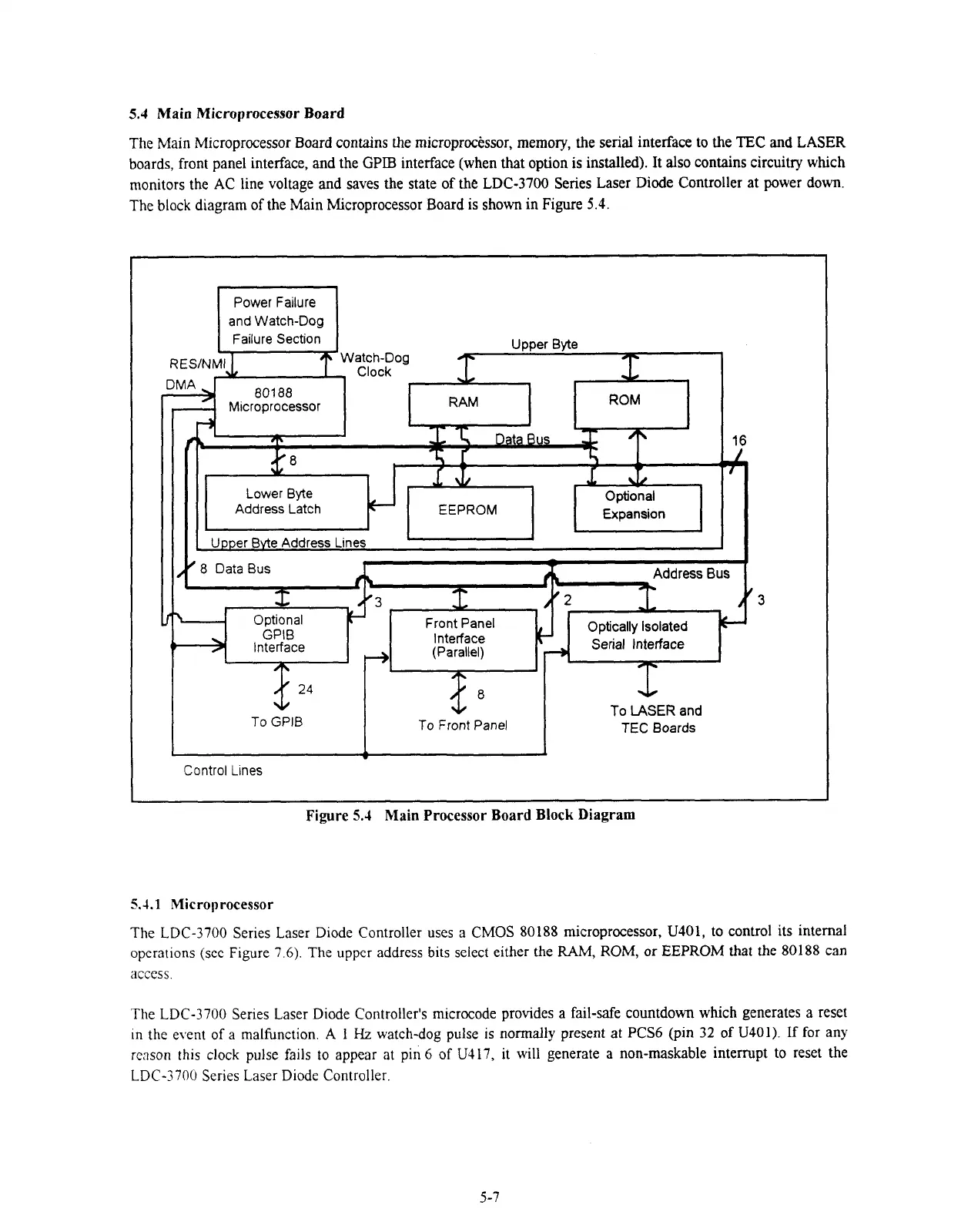
5.4
Main Microprocessor Board
Optional
Address Latch
Expansion
_
Upper Byte Address Lines
8
Data Bus
rb
Address
Bus
x
.'3
,/
2
//3
1
Optional
t.
-
Front Panel
GPlB
k
Optically Isolated
Interface
Interface (Parallel) Serial Interface
24
To
LASER
and
To GPlB To Front Panel TEC
Boards
The Main Microprocessor Board contains the microprockssor, memory, the serial interface to the
TEC
and
LASER
boards, front panel interface, and the
GPIB
interface (when that option is installed). It also contains circuitry which
monitors the AC line voltage and saves the state of the LDC-3700 Series Laser Diode Controller at power down.
The block diagram of the Main Microprocessor Board is shown in Figure
5.4.
Power Failure
and Watch-Dog
Failure Section
Upper Byte
RES/NMI
Watch-Dog
.
Clock
DMA
801
88
I
'
Microprocessor
RAM
I
ROM
J
1
.
Control Lines
Figure
5.4
Main Processor Board Block Diagram
5.4.1
Microprocessor
The LDC-3700 Series Laser Diode Controller uses a CMOS 80188 microprocessor, U401, to control its internal
operations (see Figure
7.6).
The upper address bits select either the
RAM,
ROM,
or
EEPROM
that the 80188 can
access
The LDC-3700 Series Laser Diode Controller's microcode provides a fail-safe countdown which generates a reset
In the eyent
of
a malfunction.
A
1
Hz
watch-dog pulse is
normally
present at
PCS6
(pin
32
of
U401).
If
for
any
reason
this clock pulse fails to appear at pin
6
of U417, it will generate a non-maskable interrupt to reset the
LDC-3700 Series Laser Diode Controller.
Artisan Technology Group - Quality Instrumentation ... Guaranteed | (888) 88-SOURCE | www.artisantg.com
 Loading...