To configure the FPGA with a test system design, follow these steps:
1. On the Configure menu, click the Configure command that corresponds to the
functionality you want to test.
2. In the dialog box that appears, click Configure to download the corresponding
design's SRAM Object File (.sof) to the FPGA. The download process usually
takes less than a minute.
When configuration is completed, the design begins running in the FPGA. The
corresponding GUI application tabs that interface with the design is now enabled. If
you use the Quartus Prime Programmer for configuration, instead of the BTS GUI, you
might need to restart the GUI.
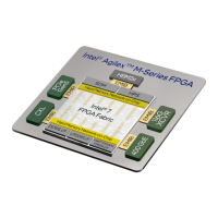
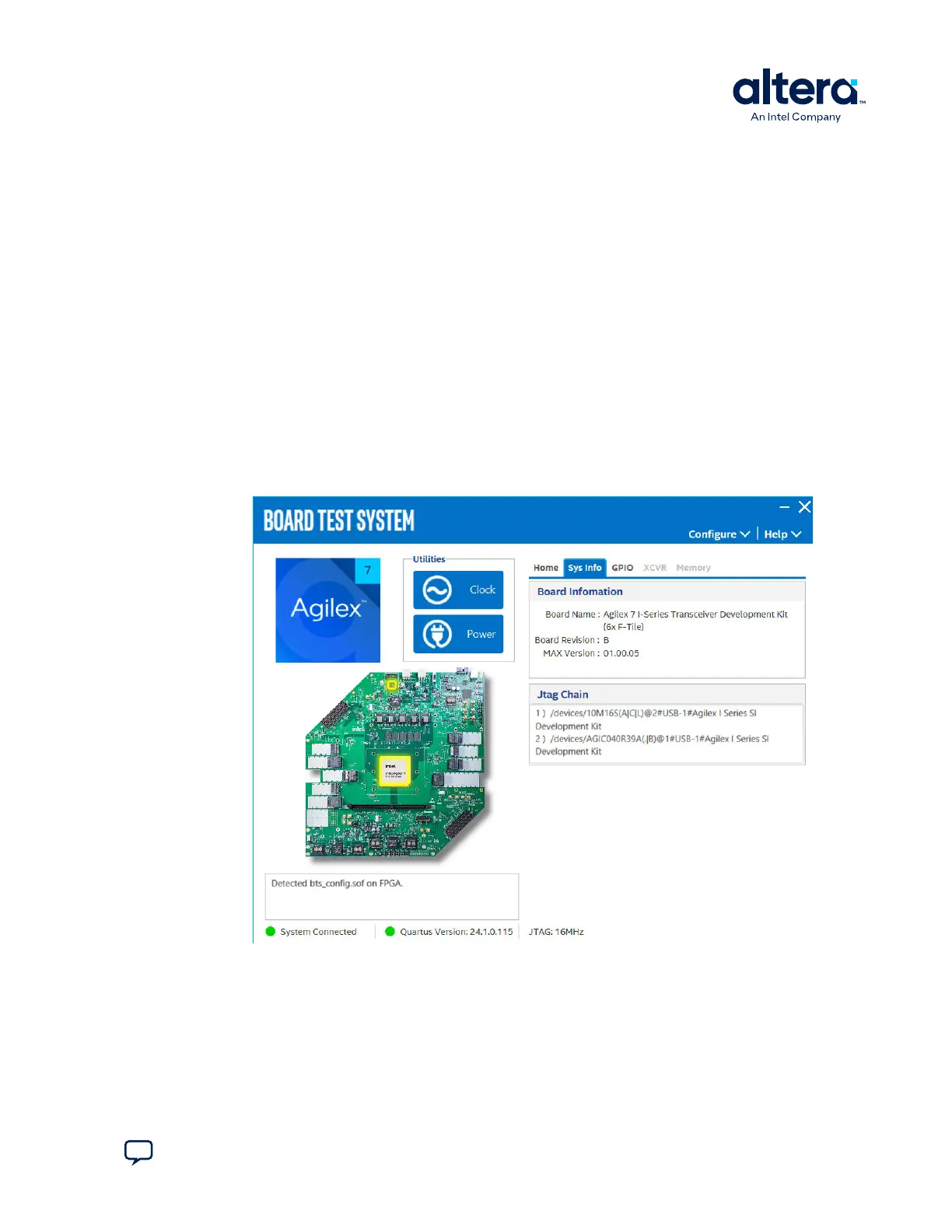
4.2.3. The Sys Info Tab
The Sys Info tab shows information about the board's current configuration. The tab
displays the board information, JTAG Chain devices and other details stored on the
board.
Figure 9. The Sys Info Tab
The following sections describe the controls on the Sys Info tab.
4. Board Test System
776646 | 2024.11.21
Send Feedback
Agilex
™
7 FPGA I-Series Transceiver (6 × F-Tile) Development Kit User Guide
19