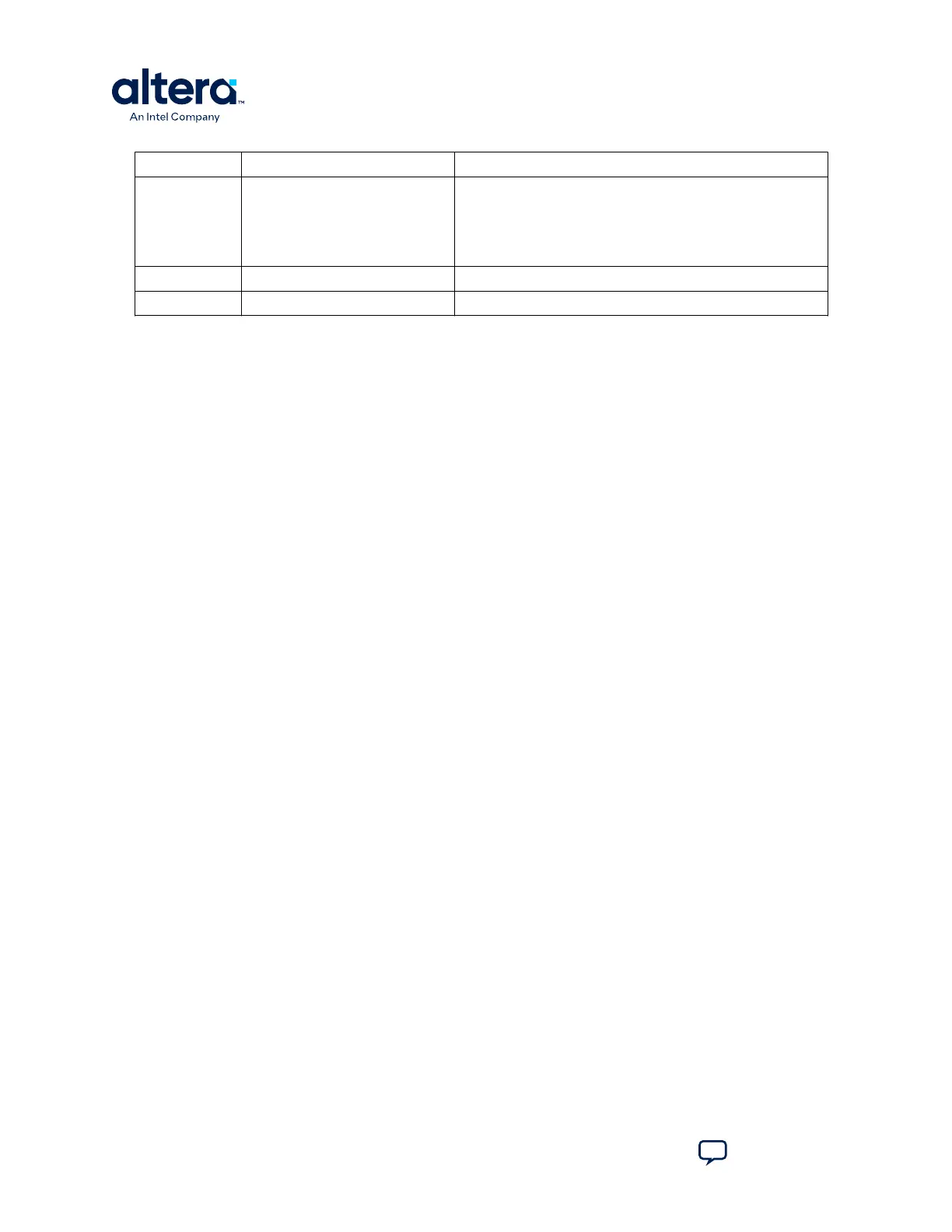
Switch Default Position Default Function
Mapped as follows:
• MUX_DIP_SW0 --> MUX_SEL0
• MUX_DIP_SW1 --> MUX_SEL1
• MUX_DIP_SW2 --> MCIO_CLK_SEL_EP_N; RP
• MUX_DIP_SW3 --> MCIO_CLK_ENN
S7 OFF Board power supply
S4 ON/ON/ON/ON Future development
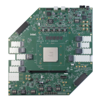
3.2. Powering Up the Development Kit
1. Use the provided 240 W power adapter to supply power through J30.
2. Connect extra 240 W adapter to J55 only when you require more than 240 W
during high use case applications.
3. After power adapter is plugged into J30, set the power switch S7 to the ON
position.
When the board powers up, the LED D22 illuminates, which indicates that the board
power up is successful. If the LED D22 is not turned on, it indicates that one or more
power supply is incorrect.
3.3. Performing Board Restore
This development kit ships with GPIO design examples stored in the QSPI flash device
and system MAX 10 pre-programmed.
You must perform board restore by using the restore menu under the BTS GUI or
using the following instructions through the Quartus Prime Programmer GUI.
3.3.1. Restoring Board System MAX 10 with Default Factory Image
1. Start the Quartus Prime Programmer GUI, and click Auto Detect to detect JTAG
chain after the system MAX 10 is restored.
2. Attach the system MAX 10 image on the system MAX 10 part.
3. Select programming options and click Program button.
Note: Once you plug Intel FPGA Download Cable between J11 and PC, the on-board Intel
FPGA Download Cable circuit is disabled automatically.
3. Development Kit Setup
776646 | 2024.11.21
Agilex
™
7 FPGA I-Series Transceiver (6 × F-Tile) Development Kit User Guide
Send Feedback
12