Hardware Manual
BMS Master 4 / 4.5
Ref.: IR14417 A 15.01.2018 Page 37/76
3.4.4.4 BALANCING RESISTORS
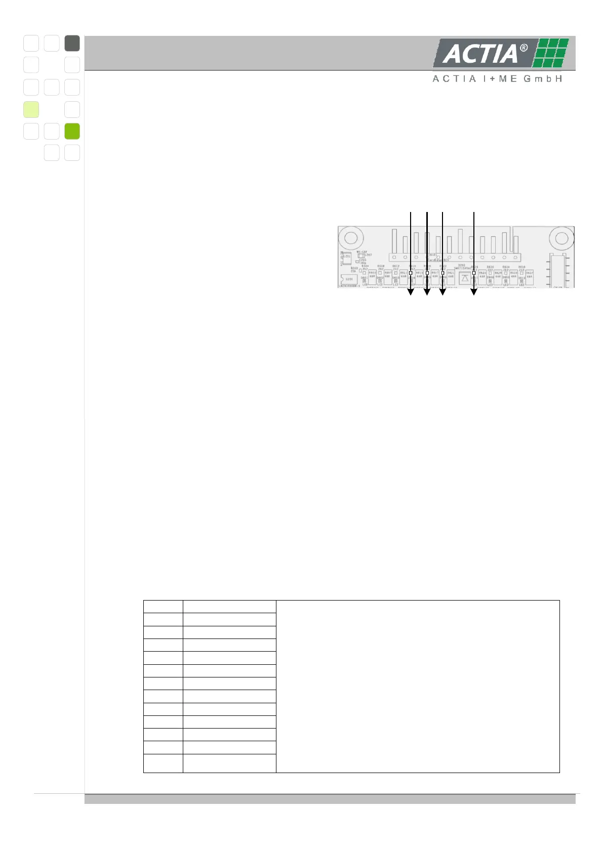
To achieve properly balanced cells a resistor of 68Ω/0.5W can be switched parallel to each
single cell to reduce the charging current with appr. 60 mA. The status of each of these
switches is visualised with 10 LEDs. Additionally, the centred four LEDs show the binary
coded Slave address after powering on the
Slave
when connecting the cell interface plug.
See sketch beside.
All balancing resistor connection points as
well as the cell connection points are lead
to
a 22-pin micro-match connector. This gives
the possibility either to connect additional
balancing resistors ≥ 47 Ω in parallel to
increase the charging currents up to 150mA
or to connect external transistors with
appropriate resistors to increase the charging current
up to 1A. In both circumstances the external balancing must be realized on a separate PCB
with adequate power dimensioning.
3.4.4.5 SERIAL RS 485 INTERFACE AND ERROR SIGNALLING
The optically isolated RS485 interface is realized with air and creeping distances of 10 mm
at least. The interface is supplied from the BMS master unit with 5 VDC.
The RS485 pins are protected against electrostatic discharge up to 15 kV (human body
model).
The interface is a 12-pin cage clamp connector (PHOENIX PTSA 2.5) with following
assignment:
(Fault Messaging Interface,
see next chapter)
Each shield input may be connected separately
to NETGND via resistor and/or capacitor in 0805
form factor below the cage clamp connector on
PCB bottom side.
Default population: both shields contacts are
shorted and connected via 10kΩ || 10 nF to
NETGND
Bit 3 Bit 2 Bit 1 Bit 0
Beispiel 1:
Beispiel 2:
0 0 1 1
0 1 1 0
= Adresse 3
= Adresse 6