PQIII Debugger | 7
©
1989-2021 Lauterbach GmbH
Target Design Requirement/Recommendations
General
• Locate the BDM/JTAG/COP connector as close as possible to the processor to minimize the
capacitive influence of the trace length and cross coupling of noise onto the JTAG signals. Don’t
put any capacitors (or RC combinations) on the JTAG lines.
• Connect TDI, TDO, TMS and TCK directly to the CPU. Buffers on the JTAG lines will add delays
and will reduce the maximum possible JTAG frequency. If you need to use buffers, select ones
with little delay. Most CPUs will support JTAG above 30 MHz, and you might want to use high
frequencies for optimized download performance.
• Ensure that JTAG HRESET
is connected directly to the HRESET of the processor. This will
provide the ability for the debugger to drive and sense the status of HRESET
. The target design
should only drive HRESET
with open collector/open drain.
• For optimal operation, the debugger should be able to reset the target board completely
(processor external peripherals, e.g. memory controllers) with HRESET
.
• In order to start debugging right from reset, the debugger must be able to control CPU HRESET
and CPU TRST
independently. There are board design recommendations to tie CPU TRST to
CPU HRESET
, but this recommendation is not suitable for JTAG debuggers.
.
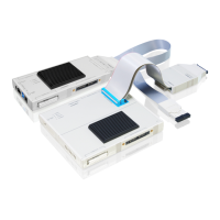
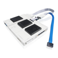
Debug cable
with blue
ribbon cable
The T32 internal buffer/level shifter will be supplied via the VCCS pin.
Therefore it is necessary to reduce the VCCS pull-up on the target board
to a value smaller 10 .