Analog signal lines
Signal input/output
RESET_N (XXXX) IO control name (register adress)
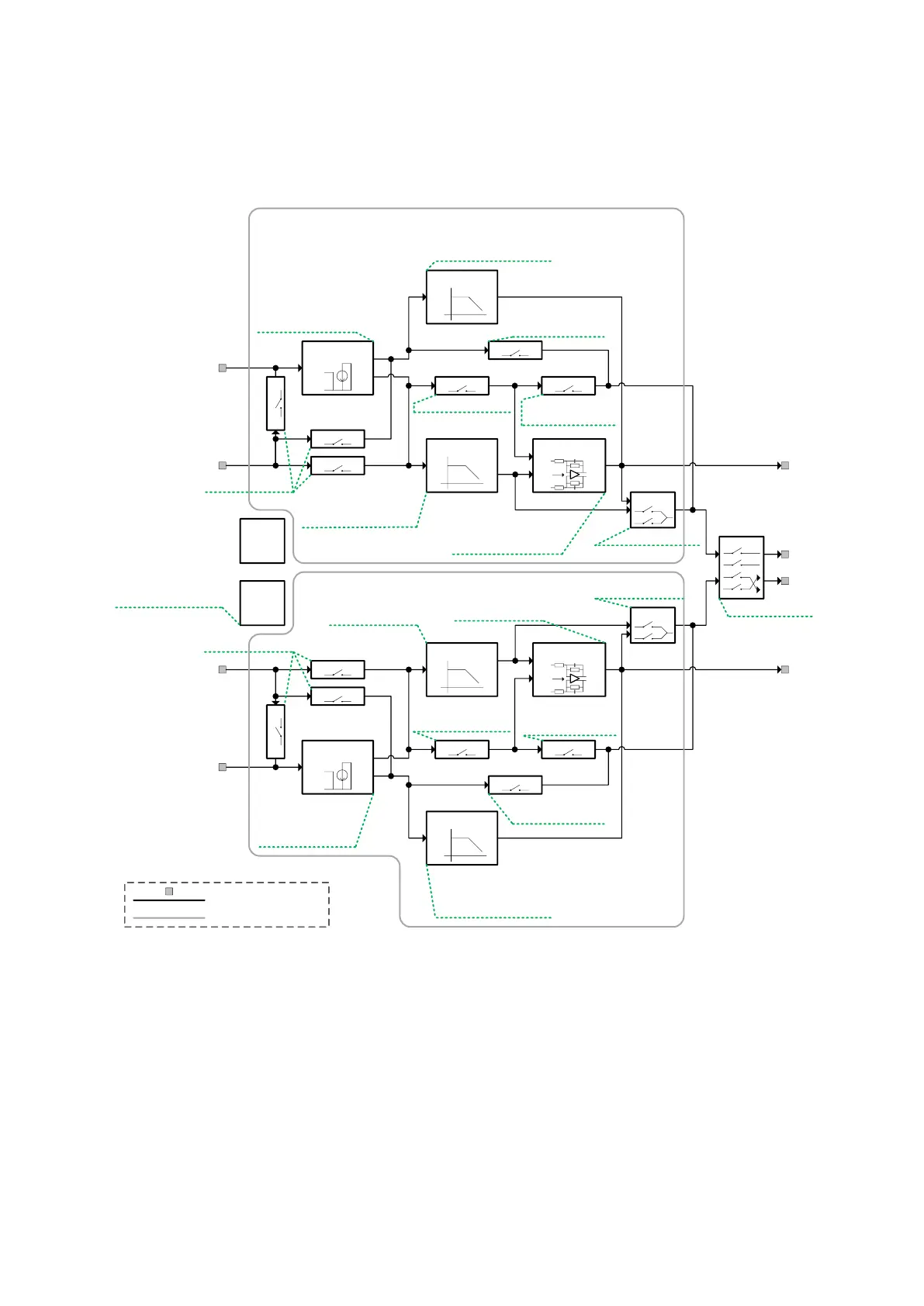
LMS7002M
TBB_TOP 1
Channel
Switch
Bias
blocks
LPF current
buffer
LPF High
LPF Low
Switch
Switch
Switch
Switch
Switch
Real pole stage
Null port
Switch
TSTIN_TBB_1 (0x010A[15:14])
EN_G_TBB_1 (0x0105[0])
STARTPULSE_TBB_1 (0x0105[15])
PD_LPFIAMP_TBB_1 (0x0105[3])
PD_LPFLAD_TBB_1 (0x0105[2])
PD_LPFS5_TBB_1 (0x0105[1])
CG_IAMP_TBB_1 (0x0108[15:10])
PD_LPFH_TBB_1 (0x0105[4])
PD_LPFLAD_TBB_1 (0x0105[2])
PD_LPFS5_TBB_1 (0x0105[1])
EN_G_TBB_1 (0x0105[0])
RCAL_LPFH_TBB_1 (0x0109[15:8])
CCAL_LPFLAD_TBB_1 (0x010A[12:8])
STARTPULSE_TBB_1 (0x0105[15])
PD_LPFLAD_TBB_1 (0x0105[2])
EN_G_TBB_1 (0x0105[0])
RCAL_LPFLAD_TBB_1 (0x0109[7:0])
CCAL_LPFLAD_TBB_1 (0x010A[12:8])
PD_LPFS5_TBB_1 (0x0105[1])
EN_G_TBB_1 (0x0105[0])
CCAL_LPFLAD_TBB_1 (0x010A[12:8])
RCAL_LPFS5_TBB_1 (0x010A[7:0])
BYPLADDER_TBB_1 (0x010A[13])
LOOPB_TBB_1 (0x0105[14:12])
PD_LPFLAD_TBB_1 (0x0105[2])
PD_LPFS5_TBB_1 (0x0105[1])
LOOPB_TBB_1 (0x0105[14:12])
PD_LPFLAD_TBB_1 (0x0105[2])
PD_LPFS5_TBB_1 (0x0105[1])
LOOPB_TBB_1 (0x0105[14:12])
Switch
LPF current
buffer
LPF High
LPF Low
Switch
Switch
Switch
Switch
Switch
Real pole stage
Null port
Switch
TSTIN_TBB_1 (0x010A[15:14])
EN_G_TBB_1 (0x0105[0])
STARTPULSE_TBB_1 (0x0105[15])
PD_LPFIAMP_TBB_1 (0x0105[3])
PD_LPFLAD_TBB_1 (0x0105[2])
PD_LPFS5_TBB_1 (0x0105[1])
CG_IAMP_TBB_1 (0x0108[15:10])
PD_LPFH_TBB_1 (0x0105[4])
PD_LPFLAD_TBB_1 (0x0105[2])
PD_LPFS5_TBB_1 (0x0105[1])
EN_G_TBB_1 (0x0105[0])
RCAL_LPFH_TBB_1 (0x0109[15:8])
CCAL_LPFLAD_TBB_1 (0x010A[12:8])
STARTPULSE_TBB_1 (0x0105[15])
PD_LPFLAD_TBB_1 (0x0105[2])
EN_G_TBB_1 (0x0105[0])
RCAL_LPFLAD_TBB_1 (0x0109[7:0])
CCAL_LPFLAD_TBB_1 (0x010A[12:8])
PD_LPFS5_TBB_1 (0x0105[1])
EN_G_TBB_1 (0x0105[0])
CCAL_LPFLAD_TBB_1 (0x010A[12:8])
RCAL_LPFS5_TBB_1 (0x010A[7:0])
BYPLADDER_TBB_1 (0x010A[13])
LOOPB_TBB_1 (0x0105[14:12])
PD_LPFLAD_TBB_1 (0x0105[2])
PD_LPFS5_TBB_1 (0x0105[1])
LOOPB_TBB_1 (0x0105[14:12])
PD_LPFLAD_TBB_1 (0x0105[2])
PD_LPFS5_TBB_1 (0x0105[1])
LOOPB_TBB_1 (0x0105[14:12])
Buffers
for SPI
signals
PD_LPFH_TBB_1 (0x0105[4])
PD_LPFIAMP_TBB_1 (0x0105[3])
PD_LPFLAD_TBB_1 (0x0105[2])
PD_LPFS5_TBB_1 (0x0105[1])
EN_G_TBB_1 (0x0105[0])
ICT_LPFS5_F_TBB_1 (0x0106[14:10])
ICT_LPFS5_PT_TBB_1 (0x0106[9:5])
ICT_LPF_H_PT_TBB_1 (0x0106[4:0])
ICT_LPFH_F_TBB_1 (0x0107[14:10])
ICT_LPFLAD_F_TBB_1 (0x0107[9:5])
ICT_LPFLAD_PT_TBB_1 (0x0107[4:0])
ICT_IAMP_FRP_TBB_1 (0x0108[9:5])
ICT_IAMP_GG_FRP_TBB_1 (0x0108[4:0])
Switch
LOOPB_TBB_1 (0x0105[14:12])
From: tbbi(p/n)_pad_1 (PAD)
From: tbbii(p/n)_1 (DAC)
From: tbbq(p/n)_pad_1 (PAD)
From: tbbiq(p/n)_1 (DAC)
To: tbboi(p/n)_1 (TX RF)
To: tbboq(p/n)_1 (TX RF)
To: txloop_1(p/n)_1 (RX BB loop)
To: txloop_2(p/n)_1 (RX BB loop)
Channel Q
Channel I
R5_LPF_BYP_TBB_1 (0x010B[0])
R5_LPF_BYP_TBB_1 (0x010B[0])