Copyright © 2011 NEXCOM International Co., Ltd. All Rights Reserved.
iii
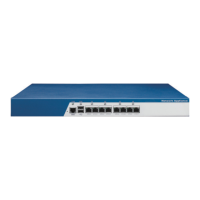
NSA 5130 User Manual
Contents
Internal Connectors ..........................................................................21
SATA2 Port .....................................................................................21
SATA3 Port .....................................................................................21
SATA4 Port .....................................................................................22
SATA Power Connector .................................................................. 22
SATA DOM Power Connector ......................................................... 23
Digital I/O Connector (4 Input, 4 Output) .......................................23
COM2 Connector ..........................................................................24
USB Connector ..............................................................................24
Parallel Interface for LCM Module ..................................................25
LCM Keypad Connector .................................................................25
HW Reset Button ...........................................................................26
Power Button ................................................................................. 26
Power Connector ...........................................................................27
GAL Programming Connector ........................................................27
System Fan (FAN1) .........................................................................28
System Fan (FAN2) .........................................................................28
CPU Fan Connector ........................................................................29
System Fan Connector ...................................................................29
PCIe Slot ........................................................................................30
PCIe Gold Finger (for LAN Module) .................................................32
Block Diagram of the Main Board .........................................................34
Chapter 3: System Setup
Removing the Chassis Cover ................................................................35
Installing a DIMM ..................................................................................36
Installing the CPU .................................................................................38
Installing a CompactFlash Card .............................................................44
Installing a 3.5” SATA Hard Drive ..........................................................46
Installing a PCI Express x8 Card .............................................................49
Replacing the LAN Module ....................................................................51
Rackmount Bracket Kit (optional) ..........................................................55
Chapter 4: BIOS Setup
BIOS Setup Utility .................................................................................. 61
Main ..................................................................................................61
Advanced ...........................................................................................62
Chipset ...............................................................................................77
Boot ...................................................................................................82
Security ..............................................................................................83
Save & Exit .........................................................................................84
Appendix A: Watchdog Timer
Watchdog Timer Setting .......................................................................85
CRFC6 (Default 0x00) ...........................................................................85
Appendix B: GPI/O Programming Guide
GPIO (J9) ...............................................................................................87
Appendix C: Bypass Specifications
Bypass Control Register Map .................................................................90
Bypass Control Register Bit Definitions ..................................................91
Appendix D: Power Consumption
Power Consumption .............................................................................93