2.4.2 Transistor (Tr) Type (NPN)
Output specifications
Item
Allowable load voltage
range
4.75 to 26.4 V DC
Max. load current 0.5 A
Max. inrush current 1.5 A
Input points per
6 points/Common 8 points/Common, 6 points/Common
Off state leakage
current
1 µA or less
On state voltage drop 0.3 V DC or less
Response
time
(at 25°C)
OFF→ON
2 µs or less (Y0 to Y3) (Load current: at 15 mA or more)
20 µs or less (C14: Y4 to Y5, C30/C60: Y4 to Y7)(Load current: at 15 mA or
more)
1 ms or less (C14: None, C30/C60: from Y8)
ON→OFF
8 µs or less (Y0 to Y3) (Load current: at 15 mA or more)
30 µs or less (C14: Y4 to Y5, C30/C60: Y4 to Y7)
(Load current: at 15 mA or more)
1 ms or less (C14: None, C30/C60: from Y8)
External power supply
(+ and – terminals)
Operating mode
indicator
LED display
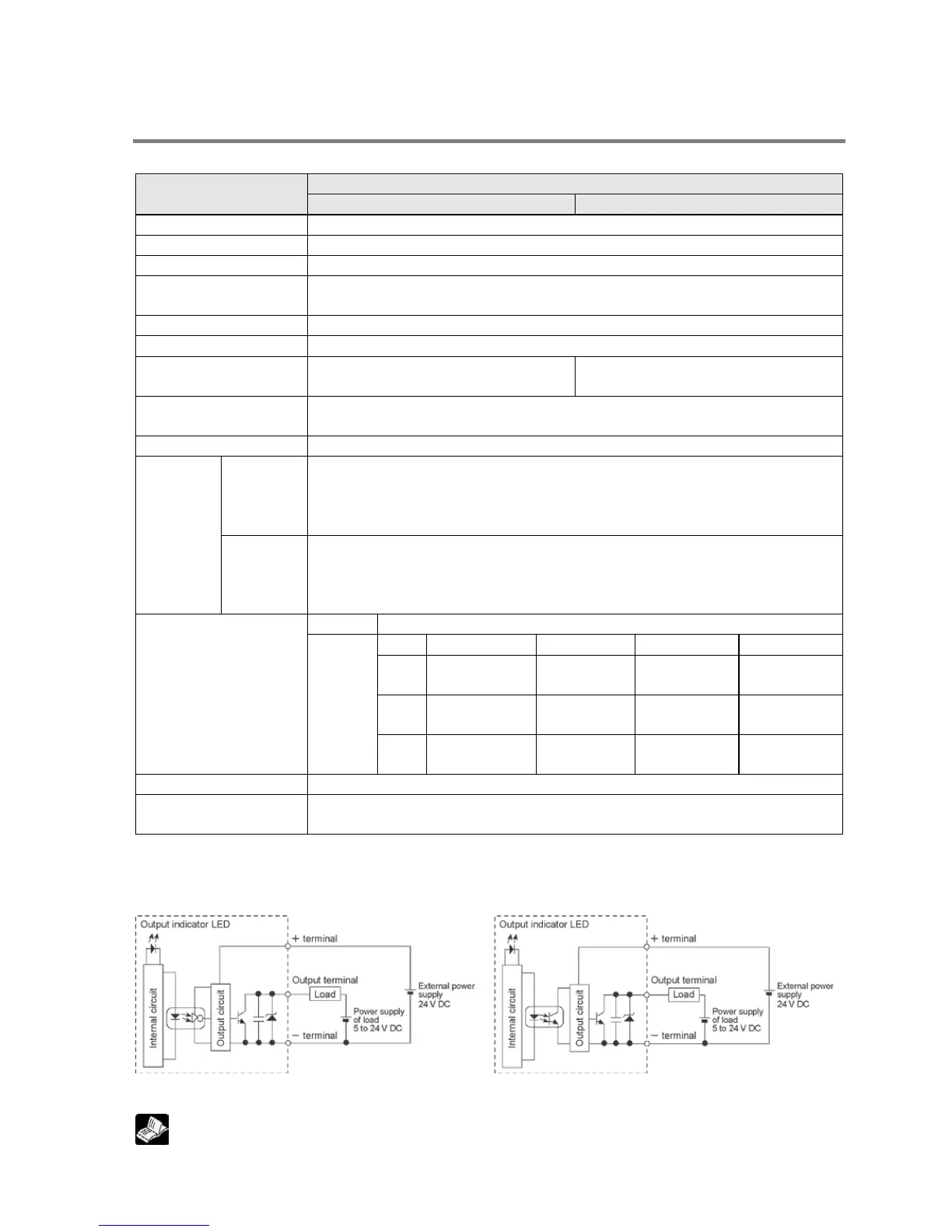
Circuit diagram
[NPN output]
[X0 to X3] [From X4]
Limitations on number of simultaneous input on points
Reference: <2.5 Limitations on Number of Simultaneous Input/Output On Points>
Phone: 800.894.0412 - Fax: 888.723.4773 - Web: www.clrwtr.com - Email: info@clrwtr.com
 Loading...