Do you have a question about the Panasonic KX-FP342CX and is the answer not in the manual?
Explains the characteristics and usage of lead-free solder in manufacturing and repair.
Details the technical specifications of the fax machine, including size, speed, and density.
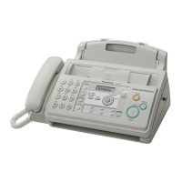
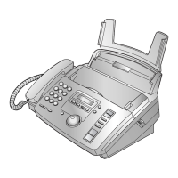
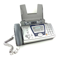
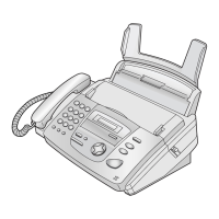
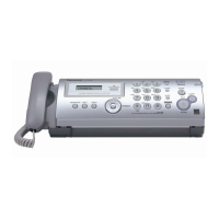
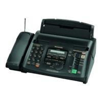
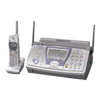
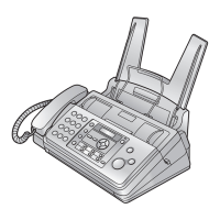
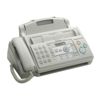
Identifies and describes the physical controls and their locations on the unit.
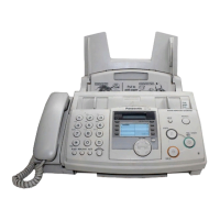
Provides instructions on connecting the handset, telephone line, and power cord.
Details the recommended space and environmental conditions for unit installation.
Outlines the maintenance procedures and identifies key component locations.
Provides troubleshooting steps for paper jams and document jams.
Describes how to clean the document feeder and thermal head.
Presents a flowchart outlining the steps for unit disassembly.
Details the step-by-step procedures for disassembling various unit components.
Lists common errors that users can resolve and their explanations.
Describes diagnostic test functions for checking unit operations.
Provides detailed information and procedures for diagnosing and resolving issues.
Provides an overview of the IC devices and their connections on the digital board.
Explains the functions of the control section, including CPU, ROM, and I/O.
Details the various sensors and switches used in the unit and their functions.
Describes the analog section's role as an interface between the telephone line and digital board.
Explains the power supply board's switching regulator method.
Provides procedures and tips for removing and replacing flat package ICs.
Illustrates the location of parts within the operation panel assembly.
Illustrates the location of parts within the back cover assembly.
Illustrates the location of parts within the upper cabinet assembly.
Illustrates the location of parts within the lower cabinet and PCB assembly.
Illustrates the location of parts within the motor assembly.
Lists replacement parts for cabinets and electrical components.
Lists replacement components for the digital board (PCB1).
Lists replacement components for the analog board (PCB2).
Lists replacement components for the operation board (PCB3).
Lists replacement components for the power supply board (PCB4).
Lists replacement components for the sensor board (PCB5).
Details the component view and bottom view of the digital board (PCB1).
Details the component view and bottom view of the analog board (PCB2).
Details the component view and bottom view of the operation board (PCB3).
Details the sensor board (PCB5) component layout.
Details the power supply board (PCB4) layout.
Schematic diagram for the analog board (PCB2).
Schematic diagram for the digital board (PCB1).
Schematic diagram for the operation board (PCB3).
Schematic diagram for the power supply board (PCB4).
Schematic diagram for the sensor board (PCB5).
| Type | Plain Paper Fax |
|---|---|
| Model | KX-FP342CX |
| Paper Size | A4, Letter |
| Paper Capacity | 50 sheets |
| Memory | 28 pages |
| Automatic Document Feeder (ADF) | Yes |
| Copier Function | Yes |
| Print Resolution | 600 x 600 dpi |
| Display | LCD |
| Fax Features | Caller ID, Delayed Transmission, Polling |
| Transmission Speed | Approximately 6 seconds per page |