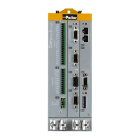
2-6 An Overview of the Drive
650V AC Drive
Functional Overview
POWER
M1 M2 M3
U
V W
Diode Bridge
Charging
Circuit
DC+
DC-
DBR-
L1
L2
L3
DBR+
DC Link
Choke
Frames
C & D
AC Line Choke
Frames E & F
PROCESSOR
CONTROL
CONTROL
TERMINALS
6521
PROGRAMMING
PORT
RS232
INTERFACE
KEYPAD
MOTOR
TERMINALS
THERMISTOR
RELAY
RL1B
RL1A
(LOCATION VARIES
WITH FRAME SIZE)
10
9
8
7
6
5
4
3
2
1
13
12
11
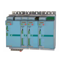
Figure 2-5 Functional Block Diagram (Frames C, D, E, F)
Power Board/Stack
DC link capacitors smooth the dc voltage output prior to the drive power stage. The IGBT
(Insulated Gate Bi-polar Transistor) output stage converts the dc input to a three phase output
used to drive the motor.
Control Board
Processor
The processor provides for a range of analog and digital inputs and outputs, together with their
reference supplies. For further details refer to Chapter 9: “Technical Specifications” - Control
Terminals.
Keypad Interface
This is a non-isolated RS232 serial link for communication with the Keypad. Alternatively, a
PC running Parker SSD Drives’ “DSE Lite” windows-based configuration software (or some
other suitable PC programming tool) can be used to graphically program and configure the
drive.
 Loading...