EasyManua.ls Logo

Profichip VPC3+S - Page 12

Default Icon
132 pages
Print Icon
To Next Page IconTo Next Page
To Previous Page IconTo Previous Page
Loading...
3 Pin Description
12
Revision 1.04
VPC3+S User Manual
Copyright © profichip GmbH, 2012
Ball
BGA
Pin
QFP
In/Out
Description
Source / Destination
D5
32
I
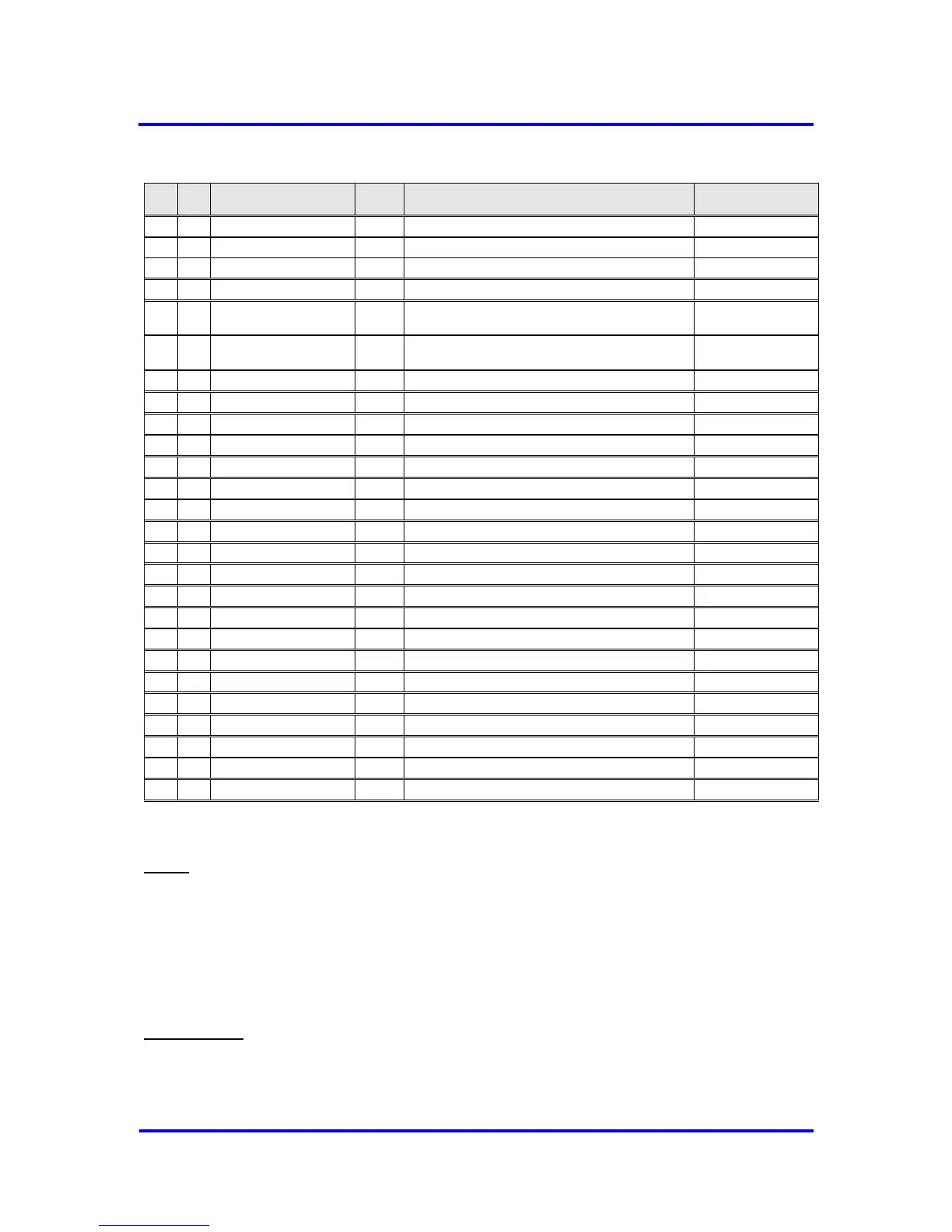
Write / E-Clock (Motorola) / Address Bus 11
CPU
D6
19
E1
31
E2
8
O
Clock Output (12 MHz or 24 MHz)
CPU / System
E3
9
I
‘0’: Parallel Interface
‘1’: Serial Interface (SPI or I2C)
Configuration Pin
E4
28
I
‘0’: Parallel Interface Intel Format
‘1’: Parallel Interface Motorola Format
Configuration Pin
E5
29
I
Test Pin 1 (to be connected to VCC)
Test Pin
E6
30
F1
10
I(S)
System Clock (48 MHz)
System
F2
11
O
Indicates state ‘Data-Exchange’ for PROFIBUS DP
LED
F3
16
I
Clear-To-Send (for FSK-Modem)
PB-Interface
F4
21
IO
Data Bus 2
CPU
F5
26
IO
Data Bus 0
CPU
F6
27
IO
Data Bus 1
CPU
G1
12
I(S)
Master-Reset (connect to port pin of CPU)
CPU
G2
15
I
Receive Data
PB-Interface
G3
17
O
Interrupt
CPU / IRQ Controller
G4
20
IO
Data Bus 7
CPU
G5
22
IO
Data Bus 4
CPU
G6
25
IO
Data Bus 3
CPU
H1
13
O
Transmit Data
PB-Interface
H2
14
O
Request-To-Send
PB-Interface
H3
42
H4
43
H5
23
IO
Data Bus 6
CPU
H6
24
IO
Data Bus 7
CPU
Figure 3-3: Pin Assignment
Notes: All signals beginning with X are LOW active.
VCC = +3.3 V
GND = 0 V
The assignment of AB11 depends on the parallel interface mode selected.
All unused inputs must be connected to GND.
Input Levels:
I :
LVTTL
I (S) :
LVTTL, Schmitt-Trigger

Table of Contents

Other manuals for Profichip VPC3+S