EasyManua.ls Logo

Profichip VPC3+S - SPI Mode; I2 C Mode

Default Icon
132 pages
Print Icon
To Next Page IconTo Next Page
To Previous Page IconTo Previous Page
Loading...
Pin Description 3
VPC3+S User Manual
Revision 1.04
17
Copyright © profichip GmbH, 2012
3.2.5 SPI Mode
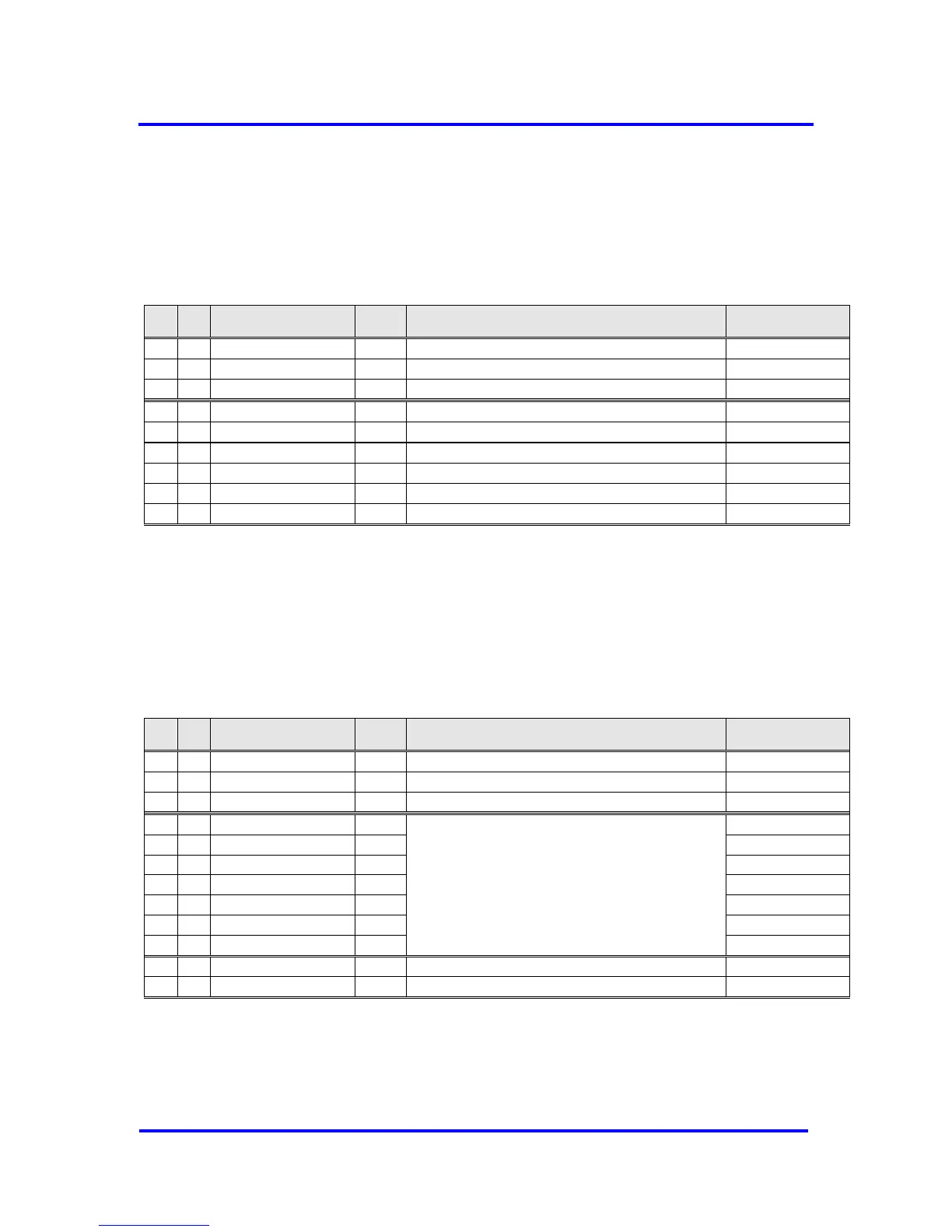
The VPC3+S can be interfaced like an SPI compatible memory device.
Depending on the setting of CPOL and CPHA four different SPI modes can
be selected. All unused inputs (including DB[7:0]) must be connected to
GND.
Ball
BGA
Pin
QFP
In/Out
Description
Connect to
E3
9
I
‘1’: Serial Interface
VCC
E4
28
I
‘0’: not used in this mode
GND
D4
33
I
‘0’: SPI Mode
GND
C2
2
I
Clock Polarity
VCC or GND
B3
44
I
Clock Phase
VCC or GND
C1
3
I
Slave-Select Signal (active low)
CPU Slave-Select
A1
48
I(S)
Serial Clock
CPU SCK
B1
1
I
Master-Out-Slave-In (Serial Data Input)
CPU MOSI
A2
47
O
Master-In-Slave-Out (Serial Data Output)
CPU MISO
Figure 3-8: Interface Configuration: SPI Mode
3.2.6 I2C Mode
The VPC3+S can be interfaced like an I2C compatible memory device. The
VPC3+S is always in slave mode, master mode is not supported. The slave
address can be configured by using the AB[6:0] inputs. All unused inputs
(including DB[7:0]) must be connected to GND.
Ball
BGA
Pin
QFP
In/Out
Description
Connect to
E3
9
I
‘1’: Serial Interface
VCC
E4
28
I
‘0’: not used in this mode
GND
D4
33
I
‘1’: I2C Mode
VCC
C3
45
I
I2C Slave Address
VCC or GND
B2
46
I
VCC or GND
B4
41
I
VCC or GND
A5
38
I
VCC or GND
A6
37
I
VCC or GND
B5
39
I
VCC or GND
B6
36
I
VCC or GND
A1
48
I(S)
Serial Clock
CPU SCK
A2
47
I(S) / O
Serial Data Line
CPU SDA
Figure 3-9: Interface Configuration: I2C Mode

Table of Contents

Other manuals for Profichip VPC3+S