Copyright © profichip GmbH, 2012
8.1.3 SPI Interface Mode
The VPC3+S is designed to interface directly with the Serial Peripheral
Interface (SPI) port of many of today’s popular microcontroller families. It
may also interface with microcontrollers that do not have a built-in SPI port
by using discrete I/O lines programmed to match the SPI protocol.
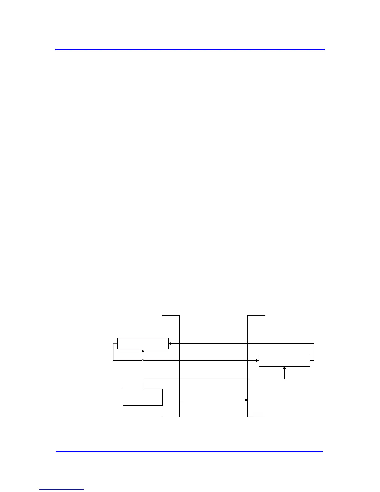
The SPI mode allows a duplex, synchronous, serial communication
between the CPU and peripheral devices. The CPU is always master while
the VPC3+S is always slave in this configuration.
Four associated SPI port pins are dedicated to the SPI function as:
Slave-Select (SPI_XSS)
Serial Clock (SPI_SCK)
Master-Out-Slave-In (SPI_MOSI)
Master-In-Slave-Out (SPI_MISO)
The clock phase control bit (SPI_CPHA) and the clock polarity control bit
(SPI_CPOL) select one of four possible clock formats to be used by the SPI
system. The CPOL bit simply selects a non-inverted or inverted clock. The
CPHA bit is used to accommodate two fundamentally different protocols by
sampling data on odd numbered SCK edges (SPI_CPHA=’0’) or on even
numbered SCK edges (SPI_CPHA=’1’).
The main element of the SPI system is the SPI Data Register. The 8-bit
data register in the master and the 8-bit data register in the slave are linked
by the MOSI and MISO pins to form a distributed 16-bit register. When a
data transfer operation is performed, this 16-bit register is serially shifted
eight bit positions by the SCK clock from the master, so data is exchanged
between the master and the slave.