Copyright © profichip GmbH, 2012
Data written to the master SPI Data Register becomes the output data for
the slave, and data read from the master SPI Data Register after a transfer
operation is the input data from the slave.
Transmission Formats
During an SPI transmission, data is transmitted (shifted out serially) and re-
ceived (shifted in serially) simultaneously. The serial clock (SCK) synchro-
nizes shifting and sampling of the information on the two serial data lines.
The slave select line allows selection of an individual slave SPI device,
slave devices that are not selected do not interfere with SPI bus activities.
The CPOL clock polarity control bit specifies an active high or low clock
and has no significant effect on the transmission format. The CPHA clock
phase control bit selects one of two fundamentally different transmission
formats. Clock phase and polarity should be identical for the master SPI
device and the communicating slave device.
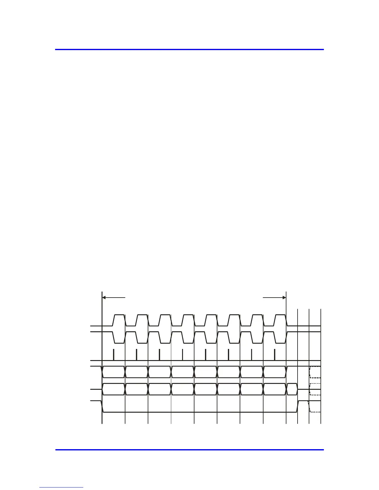
CPHA = 0 Transfer Format
The first edge on the SCK line is used to clock the first data bit of the slave
into the master and the first data bit of the master into the slave. In some
peripherals, the first bit of the slave’s data is available at the slave’s data
out pin as soon as the slave is selected. In this format, the first SCK edge is
issued a half cycle after SS has become low.
A half SCK cycle later, the second edge appears on the SCK line. When
this second edge occurs, the value previously latched from the serial data
input pin is shifted into the shift register.