Copyright © profichip GmbH, 2012
After this second edge, the next bit of the SPI master data is transmitted
out of the serial data output pin of the master to the serial input pin on the
slave. This process continues for a total of 16 edges on the SCK line, with
data being latched on odd numbered edges and shifted on even numbered
edges.
Data reception is double buffered. Data is shifted serially into the SPI shift
register during the transfer and is transferred to the parallel SPI Data
Register after the last bit is shifted in.
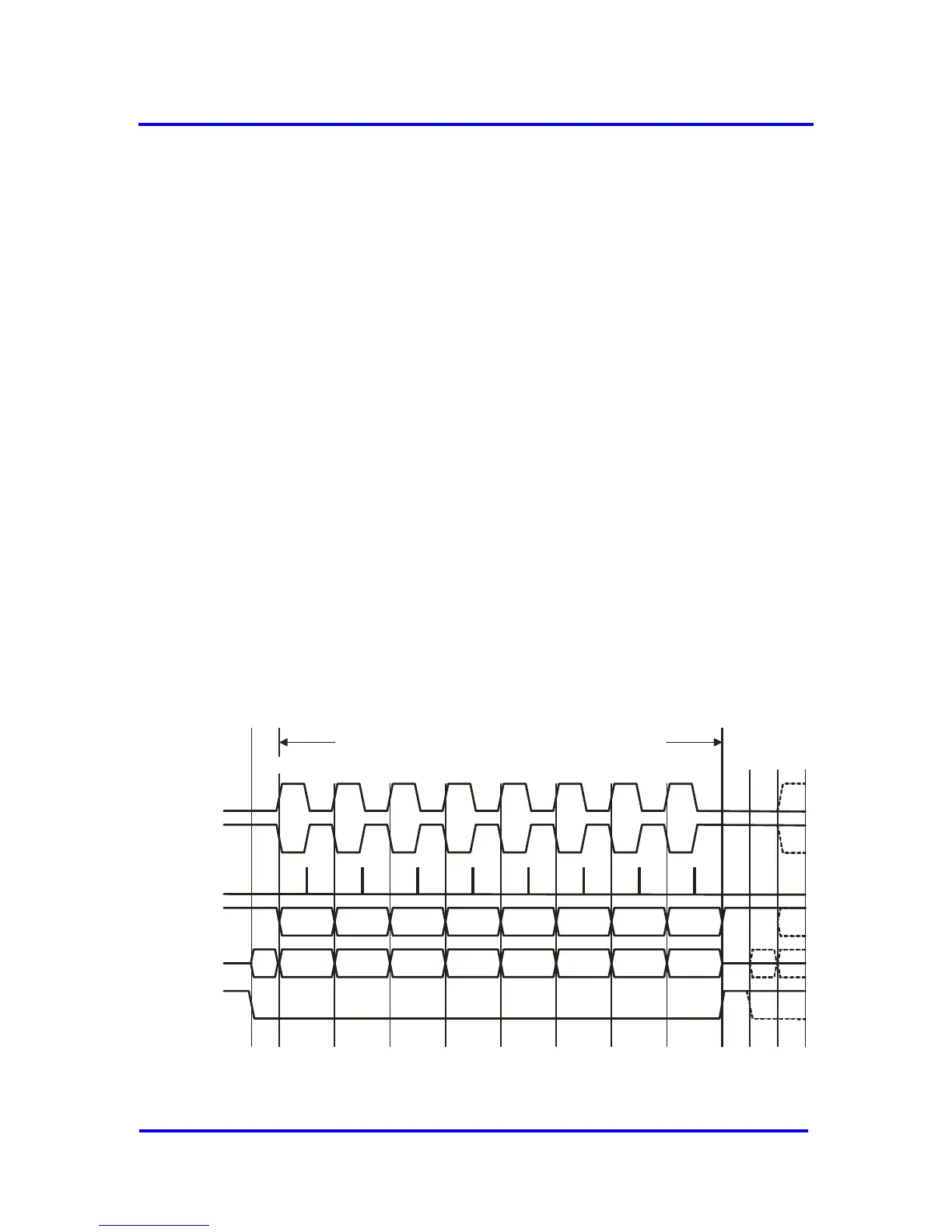
CPHA = 1 Transfer Format
Some peripherals require the first SCK edge before the first data bit
becomes available at the data out pin, the second edge clocks data into the
system. In this format, the first SCK edge is issued by setting the CPHA bit
at the beginning of the 8-cycle transfer operation.
The first edge of SCK occurs immediately after the half SCK clock cycle
synchronization delay. This first edge commands the slave to transfer its
first data bit to the serial data input pin of the master.
A half SCK cycle later, the second edge appears on the SCK pin. This is
the latching edge for both the master and slave.
When the third edge occurs, the value previously latched from the serial
data input pin is shifted into the SPI shift register. After this edge, the next
bit of the master data is coupled out of the serial data output pin of the
master to the serial input pin on the slave.