EasyManua.ls Logo

Profichip VPC3+S - Timing in the Synchronous Intel Mode

Default Icon
132 pages
Print Icon
To Next Page IconTo Next Page
To Previous Page IconTo Previous Page
Loading...
10 Operational Specifications
114
Revision 1.04
VPC3+S User Manual
Copyright © profichip GmbH, 2012
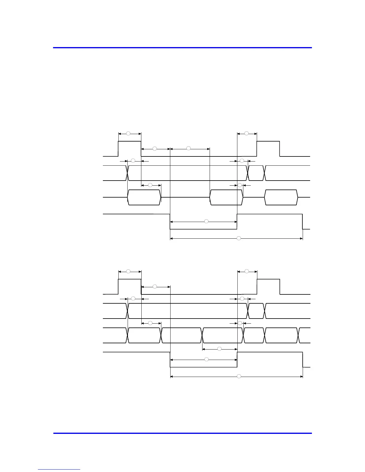
10.6.2 Timing in the Synchronous Intel Mode
In the synchronous Intel mode, the VPC3+S latches the least significant
addresses with the falling edge of ALE. At the same time, the VPC3+S
expects the most significant address bits on the address bus. An internal
chipselect signal is generated from the most significant address bits. The
request for an access to the VPC3+S is generated from the falling edge of
the read signal (XRD) and from the rising edge of the write signal (XWR).
ALE
AB10..0
DB7..0
XRD
valid
valid
data valid
address
address
1
2
3
4
5
6
10
9
8
7
Figure 10-8: Synchronous Intel Mode, READ (XWR = 1)
ALE
AB10..0
DB7..0
XWR
valid
valid
data valid
address
address
1
11
3
15
13
12
10
15
8
14
Figure 10-9: Synchronous Intel Mode, WRITE (XRD = 1)

Table of Contents

Other manuals for Profichip VPC3+S