Copyright © profichip GmbH, 2012
3.2.2 Synchronous Intel Mode
In Synchronous Intel Mode the lower 8 bits of the address lines are
multiplexed with the 8 bit data bus DB[7:0]. The upper address lines (bits
10 to 8) need to be connected to the AB[2:0] inputs of the VPC3+S.
Address line 11 is to be connected to pin C1 of the VPC3+S.
XREADY mechanism is not supported in this interface mode.
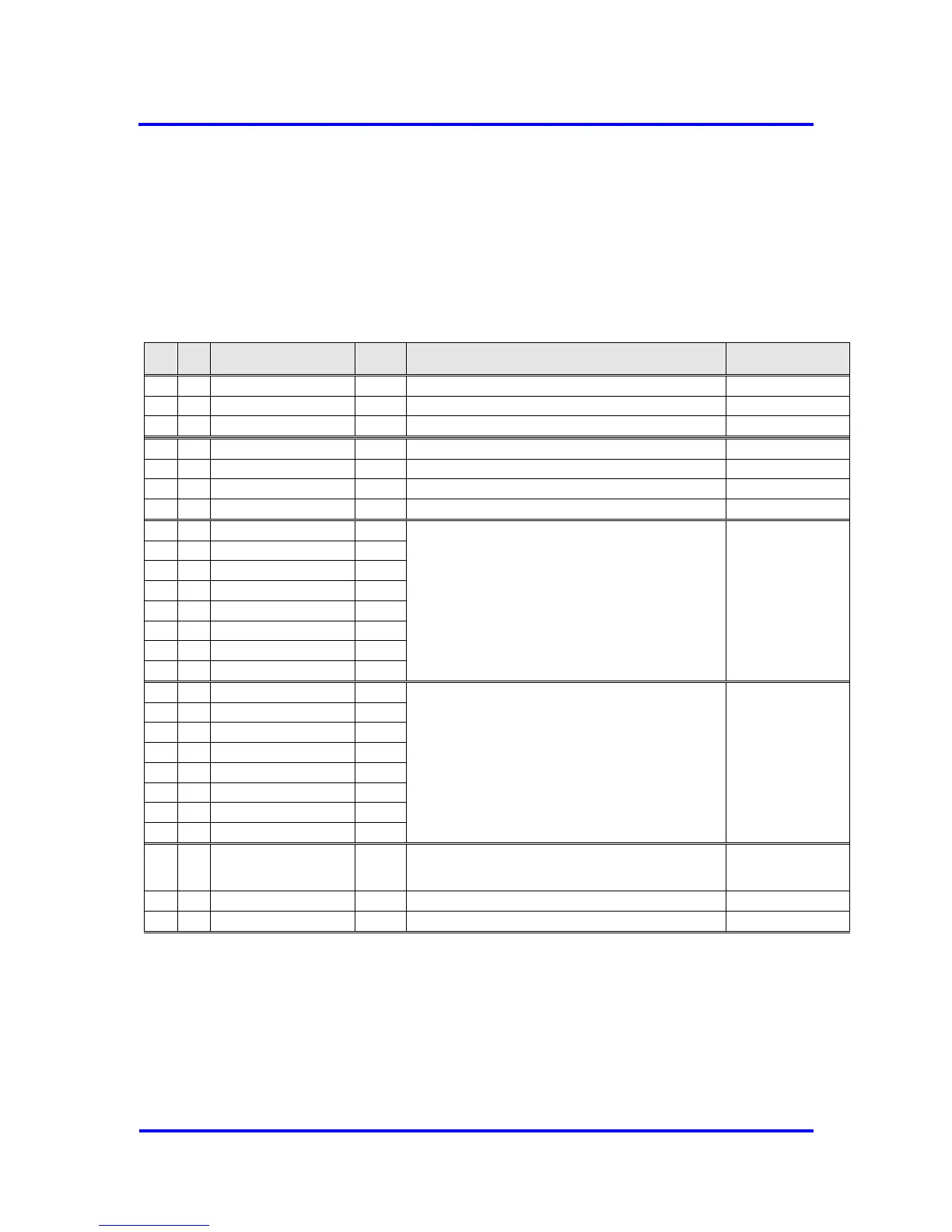
‘1’: Synchronous Interface Mode
Data Bus [7:0]
multiplexed with lower address bits [7:0]
ALE used to latch the lower address bits.
CPU Data/Address
Bus [7:0]
In Synchronous Intel Mode these inputs are used to
generate the internal Chip-Select signal.
Chip-Select is active if all inputs are ‘0’.
Use one (inverted)
CPU Address Line for
generating the
VPC3+S Chip-Select
signal.
Connect all other
inputs to GND.
Address Latch Enable
The lower address bits [7:0] are latched with the falling
edge of ALE
Write Signal (active low)
Figure 3-5: Interface Configuration: Synchronous Intel Mode