R8C/20 Group, R8C/21 Group 14. Timers
Rev.2.00 Aug 27, 2008 Page 177 of 458
REJ09B0250-0200
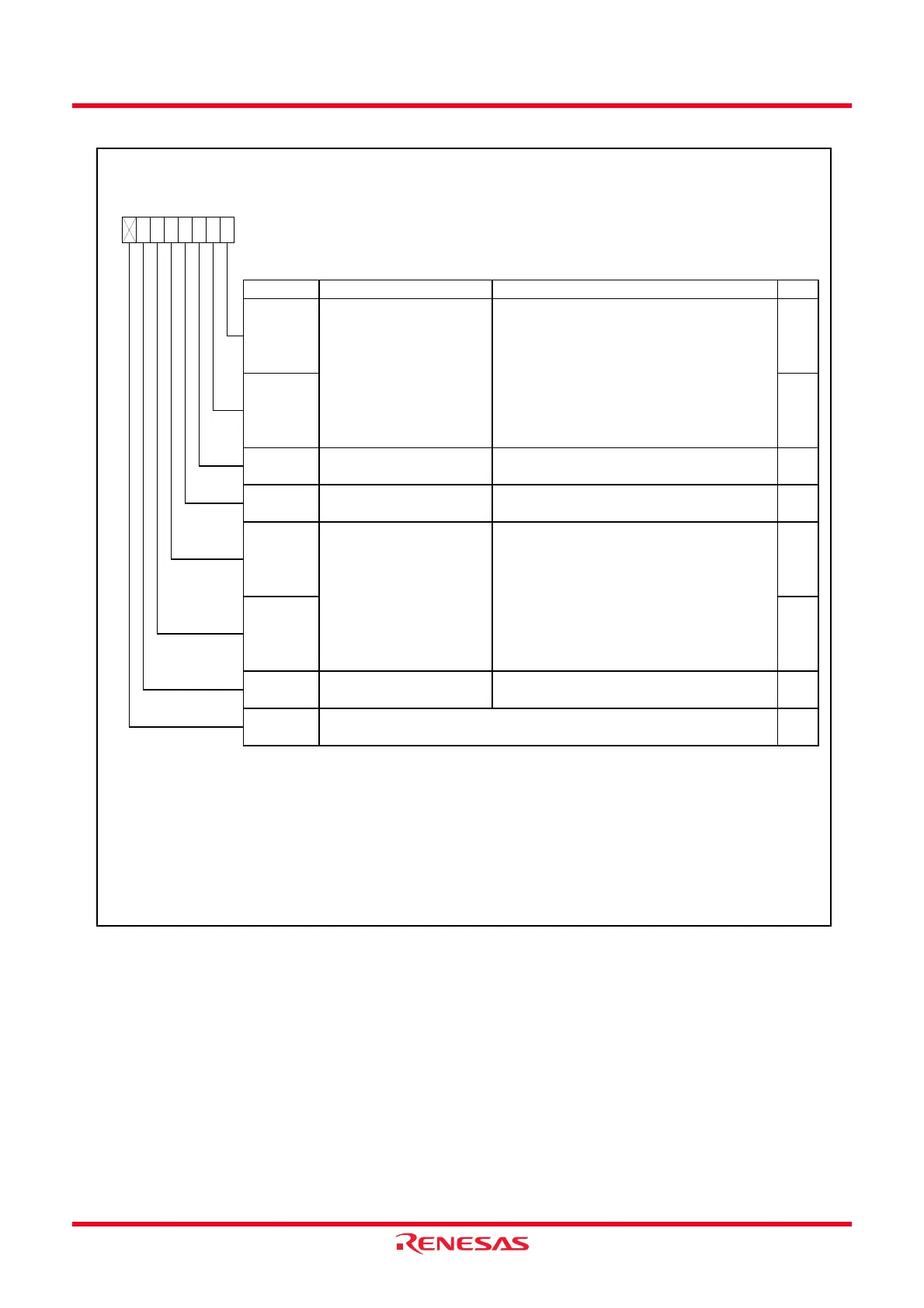
Figure 14.39 Registers TRDIORA0 to TRDIORA1 in Input Capture Function
Timer RD I/O Control Register Ai (i = 0 or 1)
Symbol Address After Reset
TRDIORA0
TRDIORA1
0141h
0151h
10001000b
10001000b
Bit Symbol Bit Name Function RW
NOTES:
1.
2.
3.
4.
Nothing is assigned. If necessary, set to 0.
When read, the content is 1.
—
IOB0
TRDGRB mode selection bit
(2)
b3 b2
IOA 3
b1 b0
1
IOA 2
1
b7 b6 b5 b4
RW
IOA 1
IOA 0
TRDGRA control bit
b1 b0
0 0 : Input capture to the TRDGRAi register
at the rising edge
0 1 : Input capture to the TRDGRAi register
at the falling edge
1 0 : Input capture to the TRDGRAi register
at both edges
1 1 : Do not set
RW
Set to 1 (input capture) in the input capture
function
When selecting 1 (The TRDGRDi register is used as a buffer register of TRDGRBi register) for this bit by the BFDi bit
in the TRDMR register, set the IOD2 bit in the TRDIORCi register to the same value as the IOB2 bit in the TRDIORAi
register.
RW
RW
—
(b7)
IOB2 RW
TRDGRB control bit
b5 b4
0 0 : Input capture to the TRDGRBi register
at the rising edge
0 1 : Input capture to the TRDGRBi register
at the falling edge
1 0 : Input capture to the TRDGRBi register
at both edges
1 1 : Do not set
The IOA3 bit in the only TRDIORA0 register is enabled. Set to the IOA3 bit in the TRDIORA1 to 1.
The IOA3 bit is enabled when the IOA2 bit is set to 1 (input capture function).
TRDGRA mode selection bit
(1)
Set to 1 (input capture) in the input capture
function
RW
Input capture input sw itch
bit
(3,4)
0 : fOCO128 Signal
1 : TRDIOA0 pin
RW
When selecting 1 (The TRDGRCi register is used as a buffer register of the TRDGRAi register) for this bit by the BFCi
bit in the TRDMR register, set the IOC2 bit in the TRDIORCi register to the same value as the IOA2 bit in the TRDIORAi
register.
IOB1
 Loading...