R8C/20 Group, R8C/21 Group 18. A/D Converter
Rev.2.00 Aug 27, 2008 Page 372 of 458
REJ09B0250-0200
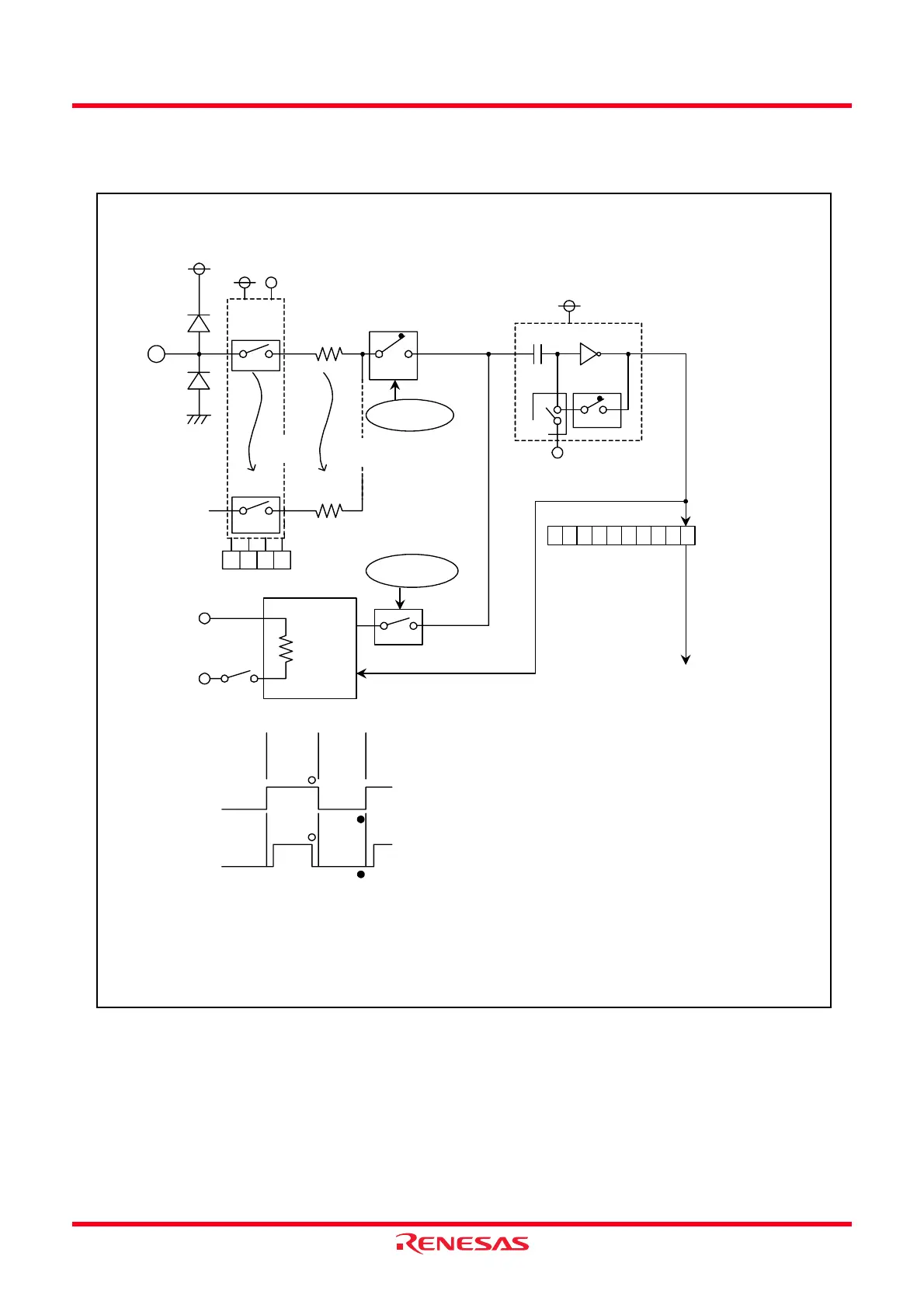
18.5 Internal Equivalent Circuit of Analog Input
Figure 18.10 shows the Internal Equivalent Circuit of Analog Input.
Figure 18.10 Internal Equivalent Circuit of Analog Input
VCC
Parasitic Diode
Chopper-type
Amplifier
A/D Successive
Conversion Register
Comparison
voltage
b1b2 b0
VCC VSS
AN0
VSS
i = 12
AN11
VREF
AVSS
Vref
Comparison reference voltage
(Vref) generator
SW1
SW2
AVCC
AMP
SW3
AVSS
VIN
SW4
SW5
SW1
Parasitic Diode
ON Resistor
Approx. 2k
Ω
Wiring Resistor
Approx. 0.2k
Ω
ON Resistor
Approx. 0.6k
Ω
ON Resistor
Approx. 2k
Ω
Wiring Resistor
Approx. 0.2k
Ω
i Ladder-type
Switches
A/D Control Register 0
ON Resistor
Approx. 0.6k f
Analog Input
Voltage
Sampling
Control Signal
ON Resistor
Approx. 5k
Ω
C = Approx.1.5pF
A/D Conversion
Interrupt Request
SW1 conducts only on the ports selected for analog input.
SW2 and SW3 are open when A/D conversion is not in progress;
their status varies as shown by the waveforms in the diagrams on the left.
SW4 conducts only when A/D conversion is not in progress.
SW5 conducts when A/D conversion is Comparison.
Control signal
for SW2
Control signal
for SW3
Sampling
Compar i son
Connect to
Connect to
Connect to
Connect to
NOTE:
1. Use only as a standard for designing this data.
Mass production may cause some changes in device characteristics.
i Ladder-type
Wiring Resistors
Resistor
ladder
Reference
Control Signal
b4
 Loading...