R8C/20 Group, R8C/21 Group 7. Programmable I/O Ports
Rev.2.00 Aug 27, 2008 Page 61 of 458
REJ09B0250-0200
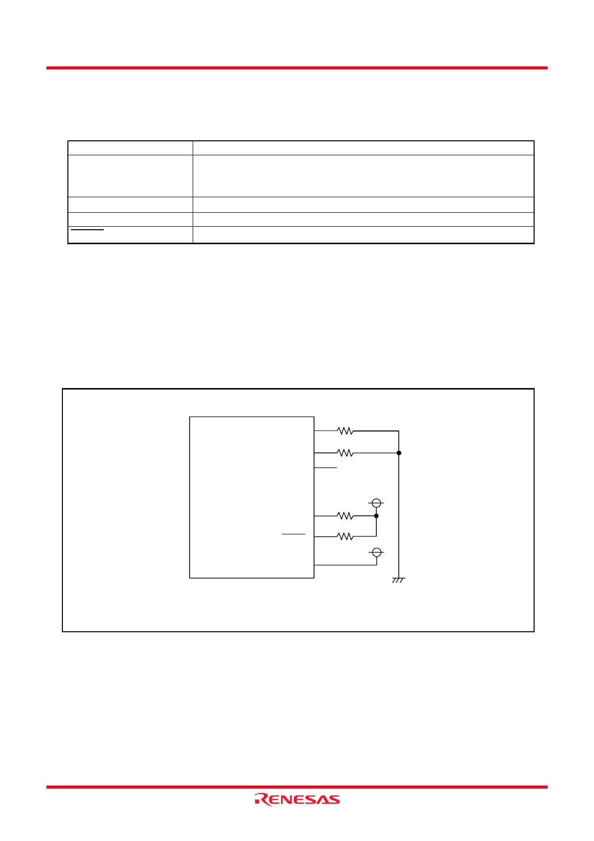
7.5 Unassigned Pin Handling
Table 7.48 lists Unassigned Pin Handling.
NOTES:
1. If these ports are set to output mode and left open, they remain input mode until they are switched to
output mode by a program. The voltage level of these pins may be undefined and the power current
may increase while the ports remain input mode.
The content of the direction registers may change due to noise or program runaway caused by
noise. In order to enhance program reliability, the program should periodically repeat the setting of
the direction registers.
2. Connect these unassigned pins to the MCU using the shortest wire length (2 cm or less) as
possible.
3. When power-on reset function is in use.
Figure 7.13 Unassigned Pin Handling
Table 7.48 Unassigned Pin Handling
Pin Name Connection
Ports P0 to P2, P3_0,
P3_1, P3_3 to P3_7,
P4_3 to P4_5, P6
• After setting to input mode, connect every pin to VSS via a resistor (pull-
down) or connect every pin to VCC via a resistor (pull-up).
(2)
• After setting to output mode, leave these pins open.
(1, 2)
Ports P4_6, P4_7
Connect to VCC via a resistor (pull-up)
(2)
Port P4_2/VREF Connect to VCC
RESET
(3)
Connect to VCC via a resistor (pull-up)
(2)
MCU
Port P0 to P2, P3_0,
P3_1, P3_3 to P3_7,
P4_3 to P4_5, P6
(Input mode )
:
:
(Input mode)
(Output mode)
Port P4_6, P4_7
RESET
(1)
Port P4_2/VREF
:
:
Open
NOTE:
1. When power-on reset function is in use.
 Loading...