R8C/20 Group, R8C/21 Group 8. Processor Mode
Rev.2.00 Aug 27, 2008 Page 62 of 458
REJ09B0250-0200
8. Processor Mode
8.1 Processor Modes
Single-chip mode can be selected as processor mode.
Table 8.1 lists Features of Processor Mode. Figure 8.1 shows the PM0 Register and Figure 8.2 shows the PM1
Register.
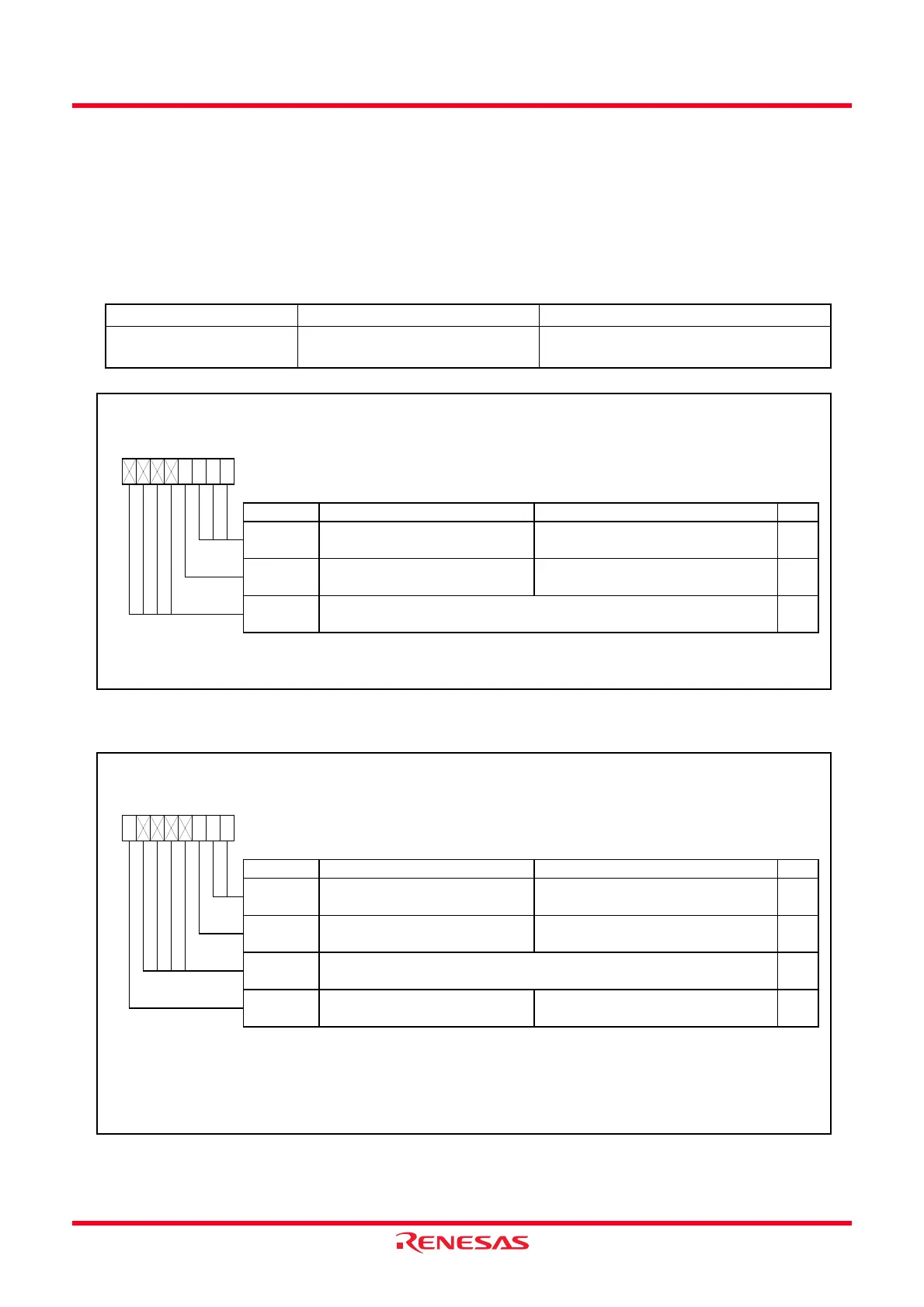
Figure 8.1 PM0 Register
Figure 8.2 PM1 Register
Table 8.1 Features of Processor Mode
Processor Mode Accessible Areas Pins Assignable as I/O Port Pins
Single-chip mode SFR, internal RAM, internal ROM All pins are I/O ports or peripheral
function I/O pins
Processor Mode Register 0
(1)
Symbol Address After Reset
PM0 0004h 00h
Bit Symbol Bit Name Function RW
NOTE:
1.
RW
Reserved bits Set to 0
Set the PRC1 bit in the PRCR register to 1 (enables w riting) before rew riting to the PM0 register.
The MCU is reset w hen this bit is set to 1.
When read, its content is 0.
RW
—
(b7-b4)
PM03
Softw are reset bit
Nothing is assigned. If necessary, set to 0.
When read, the content is 0.
b7 b6 b5 b4 b3 b2
—
b1 b0
000
—
(b2-b0)
Processor Mode Register 1
(1)
Symbol Address After Reset
PM1 0005h 00h
Bit Symbol Bit Name Function RW
NOTES :
1.
2.
0
—
(b1-b0)
RW
Reserved bits Set to 0
b7 b6 b5 b4 b3 b2
—
b1 b0
00
0 : Watchdog timer interrupt
1 : Watchdog timer reset
(2)
RW
—
(b6-b3)
PM12
WDT interrupt/reset sw itch bit
Nothing is assigned. If necessary, set to 0.
When read, the content is 0.
The PM12 bit is set to 1 by a program (it remains unchanged even if it is set to 0).
When the CSPRO bit in the CSPR register is set to 1 (selects count source protect mode), the PM12 bit is
automaticall
set to 1.
Reserved bit Set to 0
Set the PRC1 bit in the PRCR register to 1 (enables w riting) before rew riting to the PM1 register.
—
(b7)
RW
 Loading...