R8C/20 Group, R8C/21 Group 16. Clock Synchronous Serial Interface
Rev.2.00 Aug 27, 2008 Page 338 of 458
REJ09B0250-0200
16.3.5 Noise Canceller
The state of the SCL and SDA pins are routed through the noise rejection circuit before being latched internally.
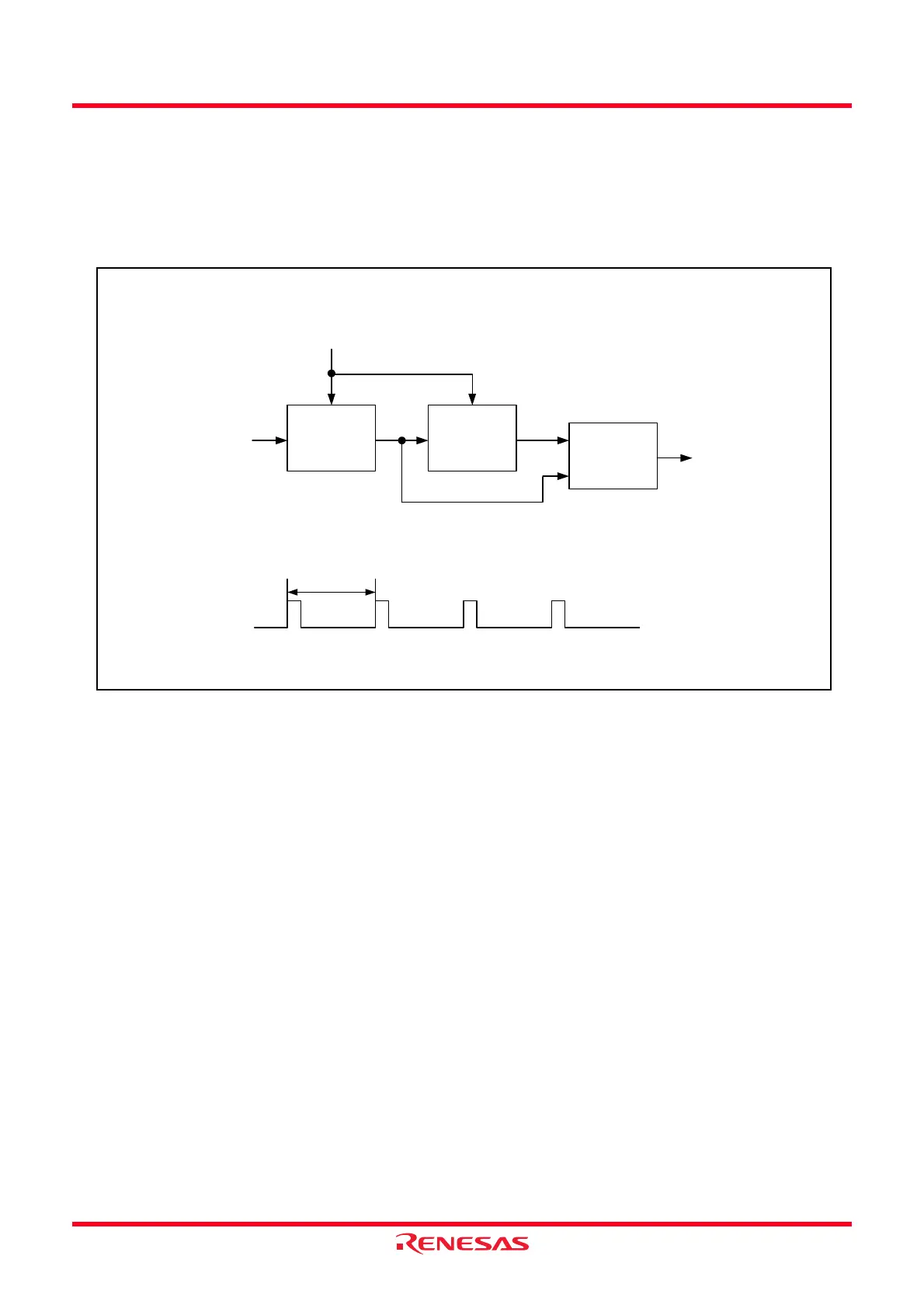
Figure 16.44 shows the Block Diagram of Noise Canceller.
The noise rejection circuit consists of two cascaded latch and match detector circuits. When the SCL pin input
signal (or SDA pin input signal) is sampled on f1 and 2 latch outputs match, the level is passed forward to the
next circuit. When they do not match, the former value is retained.
Figure 16.44 Block Diagram of Noise Canceller
C
DQ
Latch
C
DQ
Latch
Match
detection
circuit
SCL or SDA
input signal
Internal SCL
or SDA signal
f1 (sampling clock)
Period of f1
f1 (sampling clock)
 Loading...