R8C/20 Group, R8C/21 Group 18. A/D Converter
Rev.2.00 Aug 27, 2008 Page 373 of 458
REJ09B0250-0200
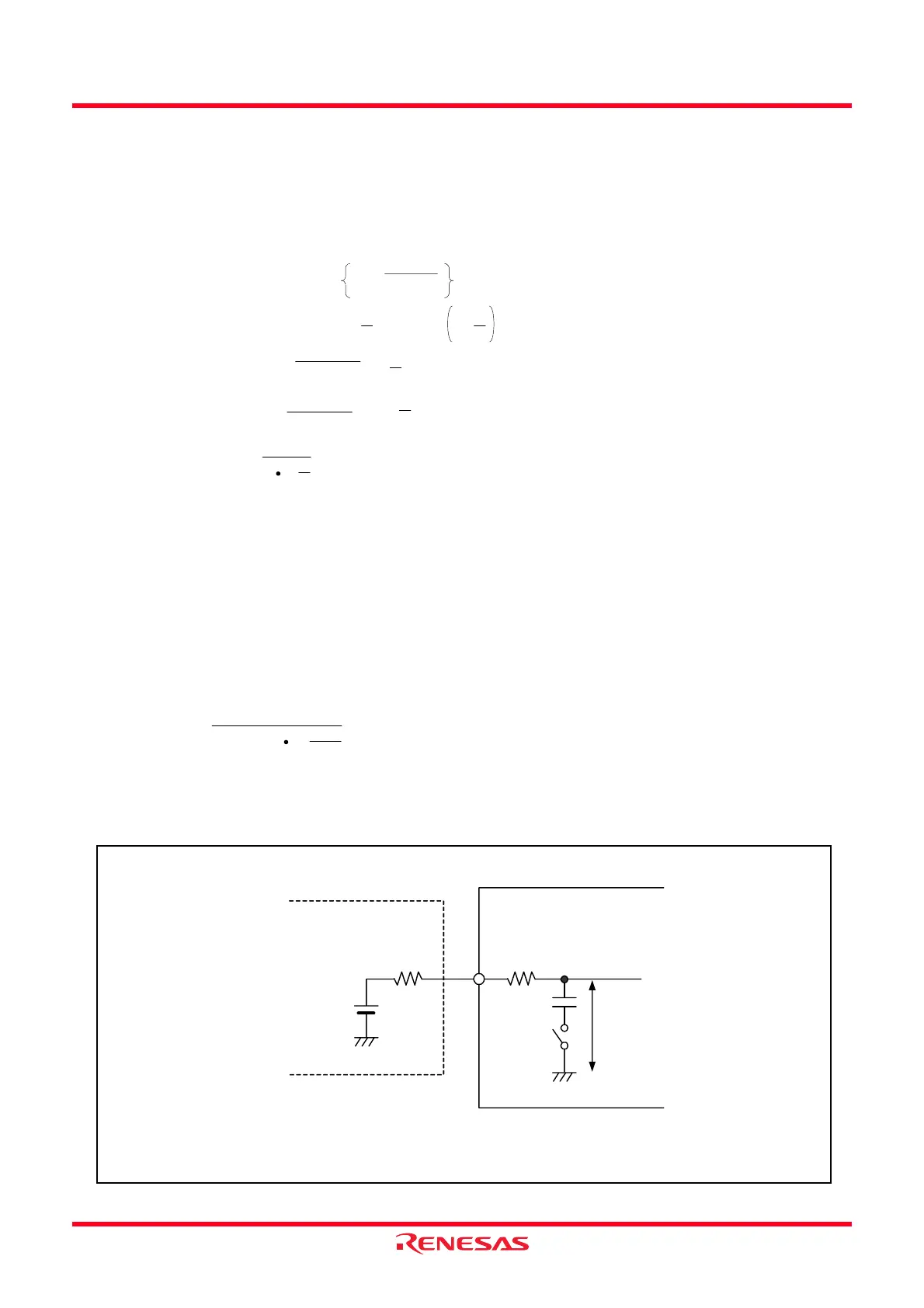
18.6 Output Impedance of Sensor Under A/D Conversion
To carry out A/D conversion properly, charging the internal capacitor C shown in Figure 18.11 has to be completed
within a specified period of time. T (sampling time) as the specified time. Let output impedance of sensor
equivalent circuit be R0, internal resistance of microcomputer be R, precision (error) of the A/D converter be X,
and the resolution of A/D converter be Y (Y is 1024 in the 10-bit mode, and 256 in the 8-bit mode).
Figure 18.11 shows Analog Input Pin and External Sensor Equivalent Circuit. When the difference between VIN
and VC becomes 0.1LSB, we find impedance R0 when voltage between pins VC changes from 0 to VIN (0.1/1024)
VIN in time T. (0.1/1024) means that A/D precision drop due to insufficient capacitor charge is held to 0.1LSB at
time of A/D conversion in the 10-bit mode. Actual error however is the value of absolute precision added to
0.1LSB.
When f(XIN) = 10 MHz, T = 0.25 µs in the A/D conversion mode without sample & hold. Output impedance R0
for sufficiently charging capacitor C within time T is determined as follows.
T = 0.25 µs, R = 2.8 kΩ, C = 6.0 pF, X = 0.1, and Y = 1024. Hence,
Thus, the allowable output impedance of the sensor equivalent circuit, making the precision (error) 0.1LSB or less,
is approximately 1.7 kΩ maximum.
Figure 18.11 Analog Input Pin and External Sensor Equivalent Circuit
VC is generally VC = VIN 1 - e
And when t = T, VC = VIN - VIN = VIN 1 -
e =
= 1n
Hence, R0 = - -R
- t
1
C(R0 + R)
X
Y
X
Y
X
Y
X
Y
- T
1
C(R0 + R)
- T
1
C(R0 + R)
T
C 1n
X
Y
R0 = -
6.0
× 10
-12
1n
0.1
1024
0.25
× 10
-6
- 2.8 × 10
3
1.7 × 10
3
~
~
MCU
Sensor equivalent circuit
R(2.8kΩ)
C(6.0pF)
R0
VIN
VC
NOTE:
1. The capacity of the terminal is assumed to be 4.5 pF
 Loading...