R8C/20 Group, R8C/21 Group 19. Flash Memory
Rev.2.00 Aug 27, 2008 Page 400 of 458
REJ09B0250-0200
19.5 Standard Serial I/O Mode
In standard serial I/O mode, the user ROM area can be rewritten while the MCU is mounted on-board by using a
serial programmer which is applicable for the MCU.
There are three types of Standard serial I/O modes:
• Standard serial I/O mode 1 . . . . Clock synchronous serial I/O used to connect with a serial programmer
• Standard serial I/O mode 2 . . . . Clock asynchronous serial I/O used to connect with a serial programmer
• Standard serial I/O mode 3 . . . . Special clock asynchronous serial I/O used to connect with a serial programmer
This MCU uses Standard serial I/O mode 2 and Standard serial I/O mode 3.
Refer to Appendix 2. Connection Examples between Serial Writer and On-Chip Debugging Emulator.
Contact the manufacturer of your serial programmer for serial programmer. Refer to the user’s manual of your
serial programmer for details on how to use it.
Table 19.7 lists the Pin Functions (Flash Memory Standard Serial I/O Mode 2), Table 19.8 lists the Pin Functions
(Flash Memory Standard Serial I/O Mode 3), Figure 19.17 shows Pin Connections for Standard Serial I/O Mode 3.
After processing the pins shown in Table 19.8 and rewriting a flash memory using a writer, apply “H” to the MODE
pin and reset a hardware if a program is operated on the flash memory in single-chip mode.
19.5.1 ID Code Check Function
The ID code check function determines whether the ID codes sent from the serial programmer and those written
in the flash memory match (refer to 19.3 Functions to Prevent Rewriting of Flash Memory).
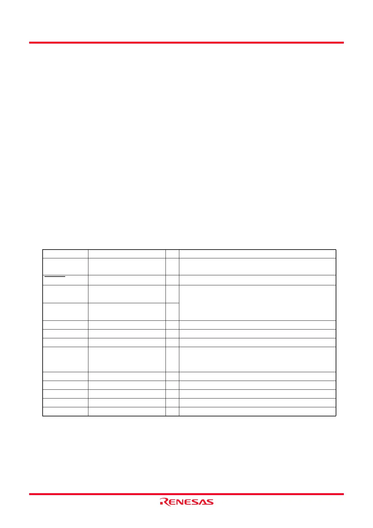
Table 19.7 Pin Functions (Flash Memory Standard Serial I/O Mode 2)
Pin Name I/O Description
VCC,VSS Power input Apply the voltage guaranteed for programming and
erasure to the VCC pin and 0 V to the VSS pin.
RESET
Reset input I Reset input pin.
P4_6/XIN P4_6 input/clock input I Connect a ceramic resonator or crystal oscillator
between the XIN and XOUT pins.
P4_7/XOUT P4_7 input/clock output I/O
P0_0 to P0_7 Input port P0 I Input “H” or “L” level signal or leave the pin open.
P1_0 to P1_7 Input port P1 I Input “H” or “L” level signal or leave the pin open.
P2_0 to P2_7 Input port P2 I Input “H” or “L” level signal or leave the pin open.
P3_0, P3_1,
P3_3 to P3_5,
P3_7
Input port P3 I Input “H” or “L” level signal or leave the pin open.
P4_2, P4_5 Input port P4 I Input “H” or “L” level signal or leave the pin open.
P6_0 to P6_5 Input port P6 I Input “H” or “L” level signal or leave the pin open.
MODE MODE I Input “L”.
P6_6 TXD output O Serial data input pin.
P6_7 RXD input I Serial data output pin.
 Loading...