R8C/20 Group, R8C/21 Group 18. A/D Converter
Rev.2.00 Aug 27, 2008 Page 367 of 458
REJ09B0250-0200
18.2 Repeat Mode
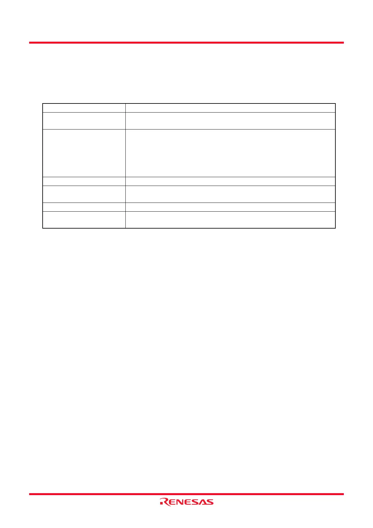
In repeat mode, the input voltage on one selected pin is A/D converted repeatedly.
Table 18.3 lists the Repeat Mode Specifications. Figure 18.6 shows the ADCON0 Register in Repeat Mode and
Figure 18.7 shows the ADCON1 Register in Repeat Mode.
Table 18.3 Repeat Mode Specifications
Item Specification
Function The Input voltage on one pin selected by CH2 to CH0 and ADGSEL0 bits
is A/D converted repeatedly
Start Condition • When the ADCAP bit is set to 0 (software trigger)
Set the ADST bit to 1 (A/D conversion starts)
• When the ADCAP bit is set to 1 (starts in timer RD (complementary PWM
mode)),
The compare match in the TRD0 and TRDGRA0 registers or the TRD1
underflow is generated while the ADST bit is set to 1
Stop Condition Set the ADST bit to 0
Interrupt Request
Generation Timing
Not generated
Input Pin Select one of AN0 to AN11
Reading of Result of A/D
Converter
Read the AD register

 Loading...