R8C/20 Group, R8C/21 Group 17. Hardware LIN
Rev.2.00 Aug 27, 2008 Page 347 of 458
REJ09B0250-0200
17.3 Register Configuration
The hardware LIN contains the following registers.
• LIN Control Register (LINCR)
• LIN Status Register (LINST)
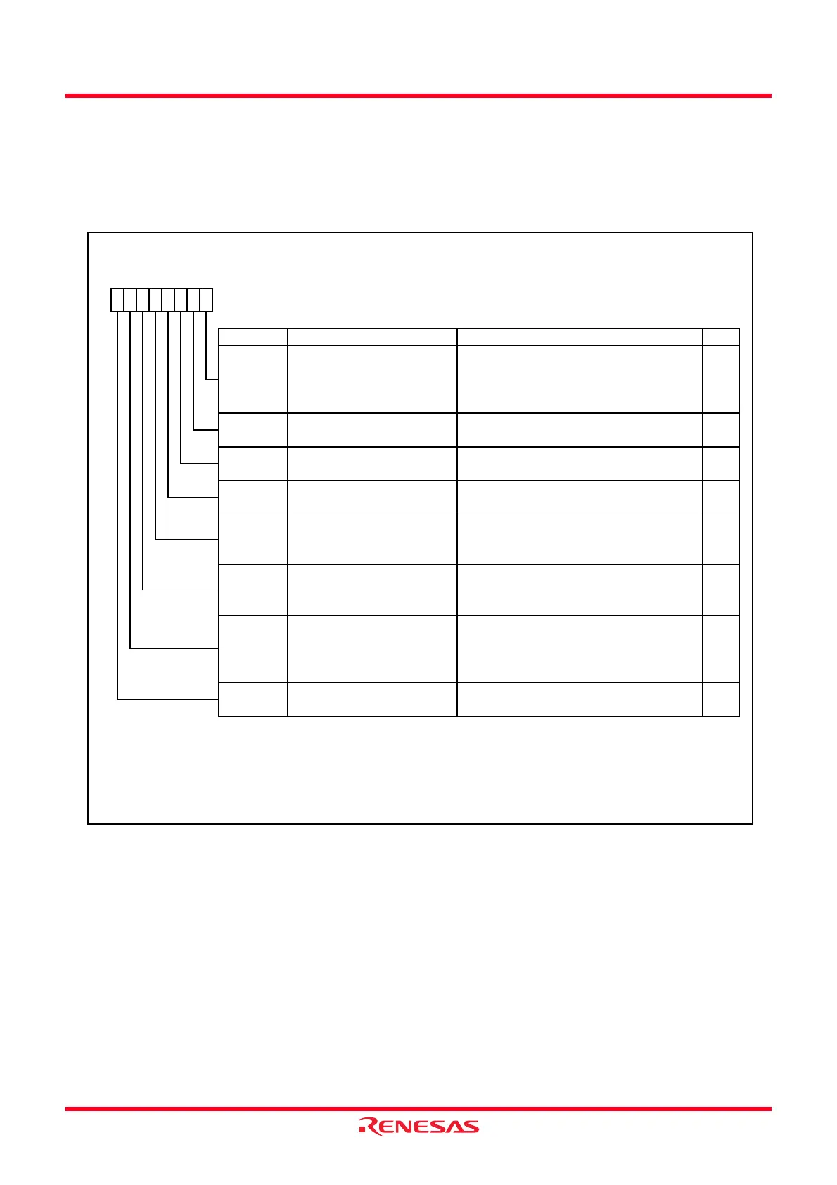
Figure 17.2 and Figure 17.3 show the LINCR and LINST Registers.
Figure 17.2 LINCR Register
LIN Control Register
Symbol Address After Reset
LINCR
0106h 00h
Bit Symbol Bit Name Function RW
NOTES:
1.
2.
3. Input to timer RA and UART0 are prohibited immediately after the LINE bit is set to 1(Causes LIN to start operating).
Ref er to
Figure 17.5 Example of Header Field Transmission Flowchart (1)
and
Figure 17.9 Example of
Header Field Rece
tion Flowchart
2
.
After setting the LSTART bit, confirm that the RXDSF flag is set to 1 before Synch Break input starts.
SBIE
BCIE
RXDSF
LSTART
0 : Unmasked after Synch Break is detected
1 : Unmasked after Synch Field measurement
is completed
Synch Break detection interrupt
enable bit
0 : Disables bus collision detection interrupt
1 : Enables bus collision detection interrupt
0 : RXD0 input enabled
1 : RXD0 input disabled
When this bit is set to 1, Timer RA input is
enabled and RXD0 input is disabled.
When read, its content is 0.
RxD0 input status flag
Synch Break detection start bit
(1)
SFIE
0 : Disables Synch Break detection interrupt
1 : Enables Synch Break detection interrupt
0 : Disables Synch Field measurement-
completed interrupt
1 : Enables Synch Field measurement-
completed interrupt
RW
RW
RW
WO
RO
RW
RxD0 input unmasking timing
select bit
(effective in only slave mode)
b3 b2 b1 b0
SBE
Bus collision detection interrupt
enable bit
b7 b6 b5 b4
Before changing LIN operation modes, temporarily stop the LIN operation (LINE bit = 0).
Synch Field measurement-
completed interrupt enable bit
MST RW
LINE
LIN operation start bit 0 : Causes LIN to stop
1 : Causes LIN to start operating
(3)
RW
LIN operation mode setting bit
(2)
0 : Slave mode
(Synch Break detection circuit actuated)
1 : Master mode
(timer RA output OR’ed w ith TxD0)
 Loading...