R8C/20 Group, R8C/21 Group 16. Clock Synchronous Serial Interface
Rev.2.00 Aug 27, 2008 Page 337 of 458
REJ09B0250-0200
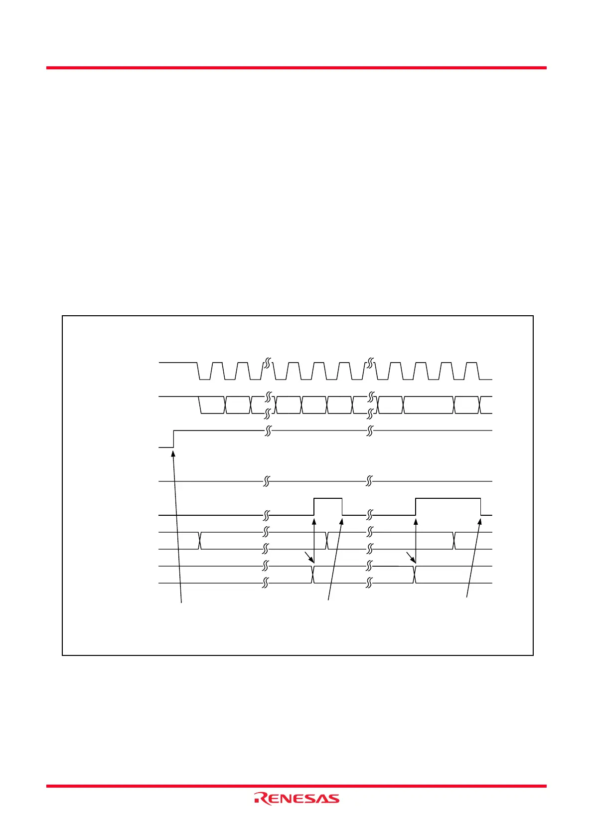
16.3.4.3 Receive Operation
In receive mode, data is latched at the rise of the transfer clock. The transfer clock is output when the MST bit
in the ICCR1 register is set to 1 and input when the MST bit is set to 0.
Figure 16.43 shows the Operating Timing in Receive Mode (Clock Synchronous Serial Mode).
The receive procedure and operation in receive mode are shown below.
(1) Set the ICE bit in the ICCR1 register to 1 (transfer operation enabled). Set the CKS0 to CKS3 bits in the
ICCR1 register and set the MST bit (initial setting).
(2) The output of the receive clock stars by setting the MST bit to 1 when the transfer clock is output.
(3) Data is transferred from the ICDRS to ICDRR registers and the RDRF bit in the ICSR register is set to
1, when the receive is completed. Since the following-byte data is enabled to receive when the MST bit
is set to 1, the continuous clock is output. The continuous receive is enabled by reading the ICDRR
register every time the RDRF bit is set to 1. An overrun is detected at the rise of the 8th clock while the
RDRF bit is set to 1, the AL bit in the ICSR register is set to 1. At this time, the former receive data is
retained in the ICDRR register.
(4) When the MST bit is set to 1, set the RCVD bit in the ICCR1 register to 1 (disables the following
receive operation) and read the ICDRR register. The SCL signal is fixed “H” after the receive of the
following-byte data is completed.
Figure 16.43 Operating Timing in Receive Mode (Clock Synchronous Serial Mode)
SDA
(input)
SCL
87
b7b1
b0
12
ICDRR register
ICDRS register
Process
by program
1781
b6 b7 b0
b6 b0
RDRF bit in
ICSR register
1
0
MST bit in
ICCR1
1
0
Data 1 Data 2
(2) Set MST bit to 1
(when transfer clock is output)
(3) Read ICDRR register
2
TRS bit in
ICCR1
1
0
Data 2 Data 3Data 1
(3) Read ICDRR register
 Loading...