R8C/20 Group, R8C/21 Group 16. Clock Synchronous Serial Interface
Rev.2.00 Aug 27, 2008 Page 336 of 458
REJ09B0250-0200
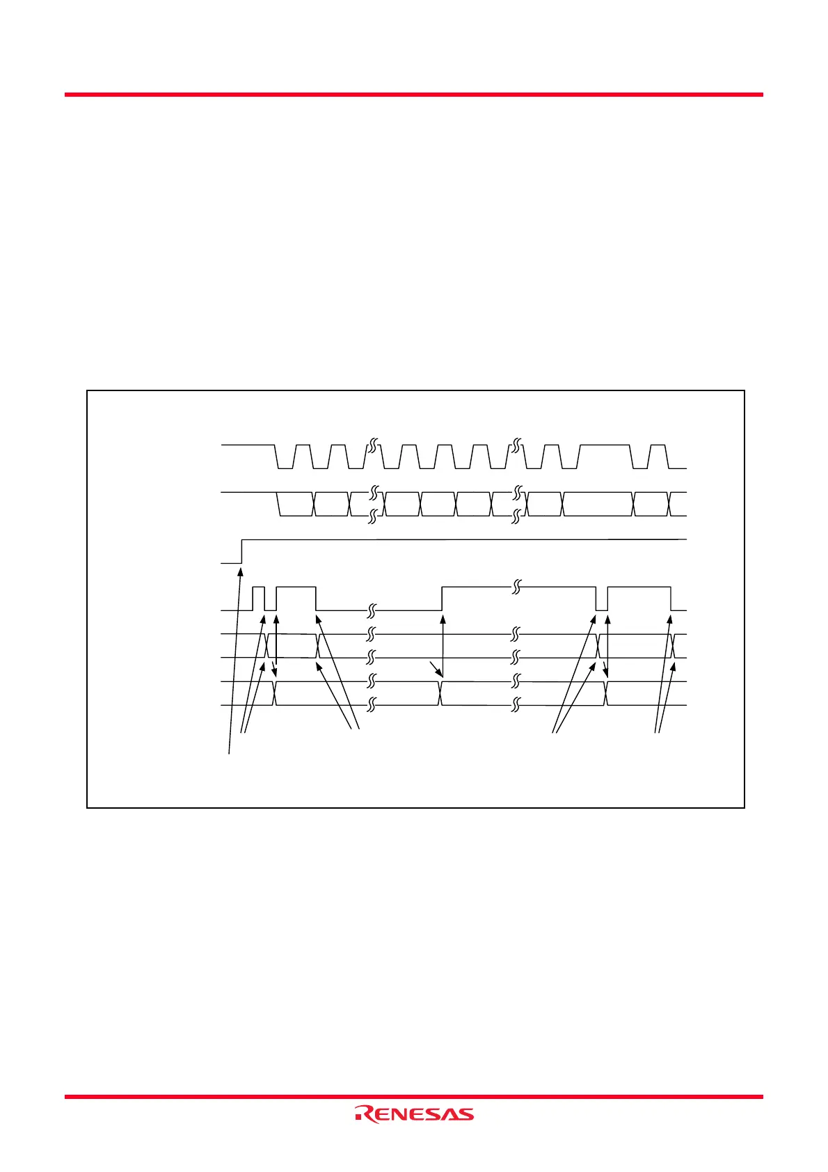
16.3.4.2 Transmit Operation
In transmit mode, transmit data is output from the SDA pin synchronizing with the fall of the transfer clock.
The transfer clock is output when the MST bit in the ICCR1 register is set to 1 and input when the MST bit is
set to 0.
Figure 16.42 shows the Operating Timing in Transmit Mode (Clock Synchronous Serial Mode).
The transmit procedure and operation in transmit mode are shown below.
(1) Set the ICE bit in the ICCR1 register to 1 (transfer operation enabled). Set the CKS0 to CKS3 bits in the
ICCR1 register and set the MST bit (initial setting).
(2) The TDRE bit in the ICSR register is set to 1 by selecting transmit mode after setting the TRS bit in the
ICCR1 register to 1.
(3) Data is transferred from the ICDRT to ICDRS registers and the TDRE bit is automatically set to 1 by
writing transmit data to the ICDRT register after confirming that the TDRE bit is set to 1. When writing
data to the ICDRT register every time the TDRE bit is set to 1, the continuous transmit is enabled. When
switching from transmit to receive modes, set the TRS bit to 0 while the TDRE bit is set to 1.
Figure 16.42 Operating Timing in Transmit Mode (Clock Synchronous Serial Mode)
SDA
(output)
SCL
87
b7b1
b0
12
ICDRT register
ICDRS register
Process
by program
1781
b6 b7 b0 b6 b0
TDRE bit in
ICSR register
1
0
TRS bit in
ICCR1 register
1
0
Data 1
Data 2 Data 3
Data 1
Data 2
Data 3
(2) Set TRS bit to 1
(3) Data write to
ICDRT register
(3) Data write to
ICDRT register
(3) Data write to
ICDRT register
(3) Data write to
ICDRT register
 Loading...