R8C/20 Group, R8C/21 Group 14. Timers
Rev.2.00 Aug 27, 2008 Page 206 of 458
REJ09B0250-0200
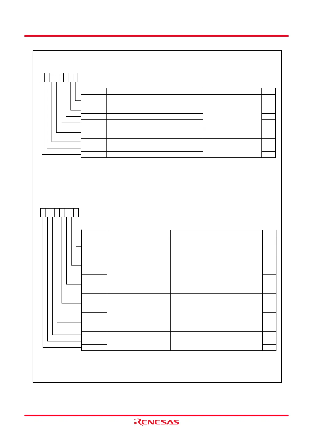
Figure 14.68 Registers TRDOCR and TRDCR0 to TRDCR1 in PWM Mode
Timer RD Output Control Register
(1)
Symbol Address After Reset
TRDOCR
013Dh 00h
Bit Symbol Bit Name Function RW
NOTES:
1.
2.
TOA1
TOB1 RW
TRDIOD1 initial output level selection bit
(2)
TRDIOB1 initial output level selection bit
(2)
TOC1 TRDIOC1 initial output level selection bit
(2)
0 : Initial output is inactive
level
1 : Initial output is active level
Set this bit to 0 (enable
output) in PWM mode
Write to the TRDOCR register w hen both the TSTART0 and TSTART1 bits in the TRDSTR register are set to 0 (count
stops).
TOC0 RW
RW
TRDIOA1 initial output level selection bit
RW
RW
0 : Inactive level
1 : Active level
TRDIOD0 initial output level selection bit
(2)
TOD1 RW
RW
TOB0 RW
TRDIOA0 output level selection bit Set this bit to 0 (enable
output) in PWM mode
TRDIOB0 output level selection bit
(2)
TRDIOC0 initial output level selection bit
(2)
TOA0
b7 b6 b5 b4
0
When the pin functions are w aveform output (refer to
Table 14.13
to
14.15
;
Table 14.17
to
14.19
) and the TRDOCR
register is set, the initial output level is output.
b3 b2
TOD0
b1 b0
0
Timer RD Control Register i (i = 0 or 1)
Symbol Address After Reset
TRDCR0
TRDCR1
0140h
0150h
00h
00h
Bit Symbol Bit Name Function RW
NOTES:
1.
2. This bit is enabled w hen the TCK2 to TCK0 bits are set to 101b (TRDCLK input) and the STCLK bit in the TRDFCR
register is set to 1 (external clock input enabled).
RW
CKEG1
CCLR0 RWSet to 001b (the TRDi register clear at the
compare match w ith TRDGRAi register) in PWM
mode.
TRDi counter clear selection bit
This bit is enabled w hen the STCLK bit in the TRDFCR register is set to 1 (external clock input enabled).
b3 b2
CKEG0
b1 b0
TCK2
001
b7 b6 b5 b4
RW
RW
RW
CCLR2
CCLR1 RW
Count source selection bit
b2 b1 b0
0 0 0 : f1
0 0 1 : f2
0 1 0 : f4
0 1 1 : f8
1 0 0 : f32
1 0 1 : TRDCLK input
(1)
1 1 0 : fOCO40M
1 1 1 : Do not set
External clock edge selection
bit
(2)
b4 b3
0 0 : Count at the rising edge
0 1 : Count at the falling edge
1 0 : Count at both edges
1 1 : Do not set
RW
TCK1 RW
TCK0
 Loading...