R8C/20 Group, R8C/21 Group 14. Timers
Rev.2.00 Aug 27, 2008 Page 209 of 458
REJ09B0250-0200
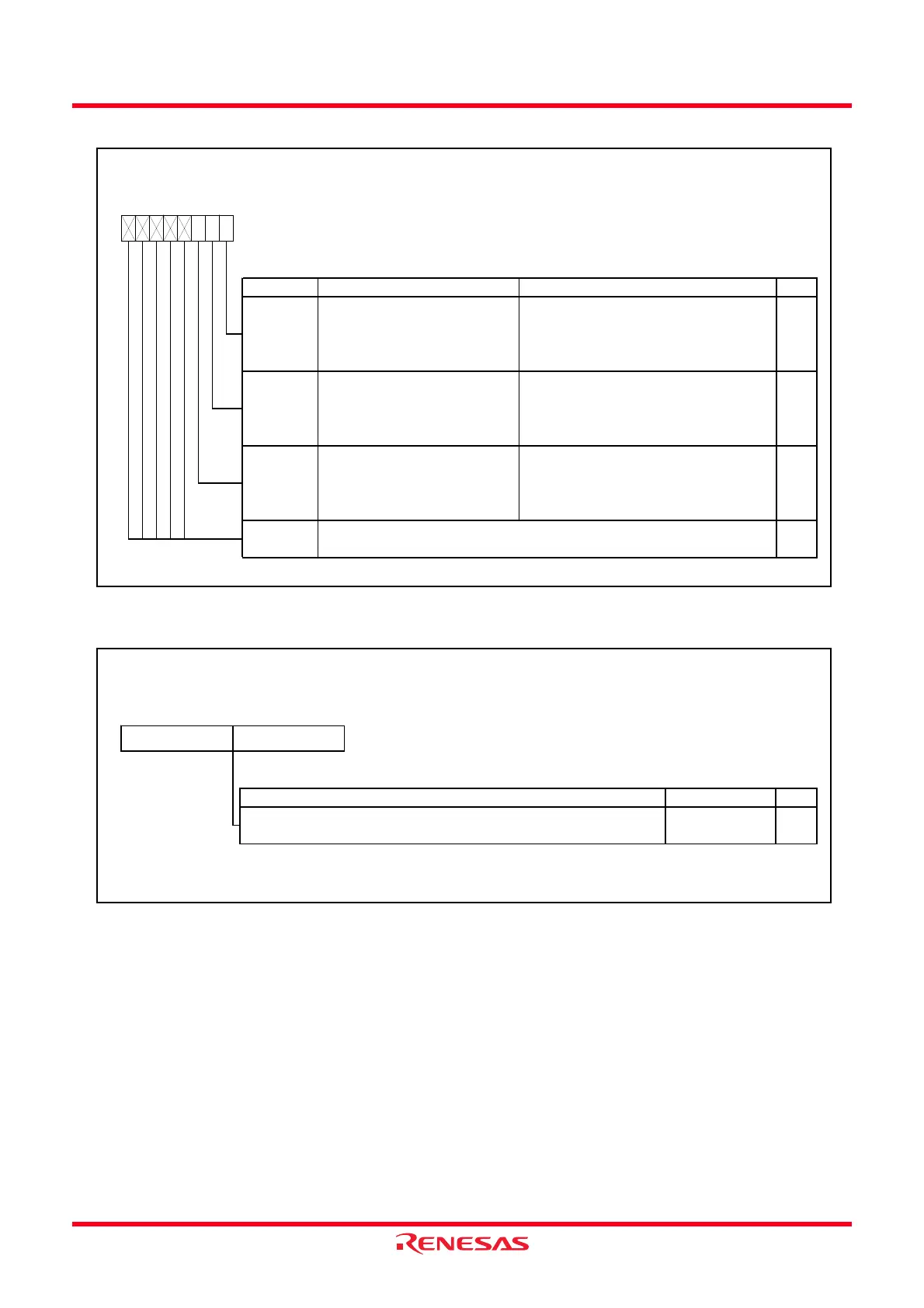
Figure 14.71 Registers TRDPOCR0 to TRDPOCR1 in PWM Mode
Figure 14.72 Registers TRD0 to TRD1 in PWM Mode
Timer RD PWM Mode Output Level Control Register i (i = 0 or 1)
Symbol Address After Reset
TRDPOCR0
TRDPOCR1
0145h
0155h
11111000b
11111000b
Bit Symbol Bit Name Function RW
b3 b2
—
(b7 - b3)
b1 b0
POLD
b7 b6 b5 b4
RW
POLC RW
PWM mode output level control bit
B
0 : “L” active of TRDIOBi output level is
selected
1 : “H” active of TRDIOBi output level is
selected
PWM mode output level control bit
C
0 : “L” active of TRDIOCi output level is
selected
1 : “H” active of TRDIOCi output level is
selected
POLB
—
Nothing is assigned. If necessary, set to 0.
When read, the content is 1.
PWM mode output level control bit
D
0 : “L” active of TRDIODi output level is
selected
1 : “H” active of TRDIODi output level is
selected
RW
Timer RD Counter i (i = 0 or 1)
(1)
Symbol Address After Reset
TRD0
TRD1
0147h-0146h
0157h-0156h
0000h
0000h
Setting Range RW
NOTE:
1.
Function
Count a count source. Count operation is incremented.
When an overflow occurs, the OVF bit in the TRDSRi register is set to 1.
0000h to FFFFh RW
Access the TRDi register in 16-bit units. Do not access it in 8-bit units.
b0b7
(b8)
b0
(b15)
b7
 Loading...