R8C/20 Group, R8C/21 Group 14. Timers
Rev.2.00 Aug 27, 2008 Page 211 of 458
REJ09B0250-0200
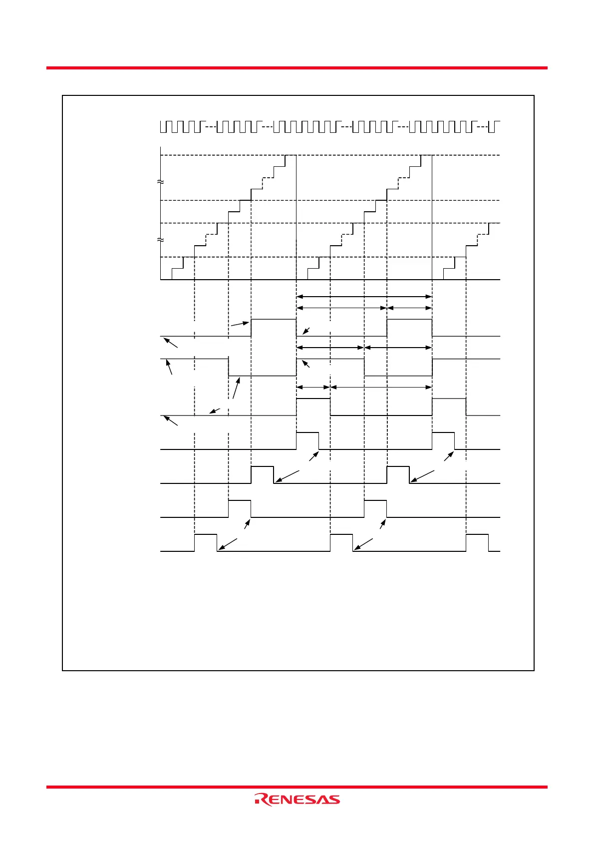
Figure 14.74 Operating Example of PWM Mode
m
n
p
Value in TRDi register
Count source
m + 1
n + 1
TRDIOCi output
q
m - n
p + 1 m - p
m - qq + 1
TRDIODi output
m: Setting value in TRDGRAi register
n: Setting value in TRDGRBi register
p: Setting value in TRDGRCi register
q: Setting value in TRDGRDi register
Inactive Level “L”Active level “H”
Inactive Level “H”
Active level “L”
Initial output “L” to
compare match
Initial output “H” to
compare match
Set to 0 by a program Set to 0 by a program
Set to 0 by a program
TRDIOBi output
IMFA bit in
TRDSRi register
1
0
IMFB bit in
TRDSRi register
1
0
IMFC bit in
TRDSRi register
1
0
IMFD bit in
TRDSRi register
1
0
i = 0 or 1
Set to 0 by a program
The above applies to the following conditions:
The BFCi and BFDi bits in the TRDMR register are set to 0. (The TRDGRCi and TRDGRDi registers are not used as the buffer register.)
The EBi, ECi and EDi bits in the TRDOER1 register are set to 0. (Enable TRDIOBi, TRDIOCi and TRDIODi pin outputs.)
The TOBi and TOCi bits in the TRDOCR register are set to 0 (inactive level), the TODi bit is set to 1. (active level)
The POLB bit in the TRDPOCRi register is set to 1 (active level “H”), the POLC and POLD bits are set to 0. (active level “L”)
Initial output “L” to
compare match
 Loading...